16 May 2008


15 May 2008
Optical communications goes nano -- HP announces practical interconnect tech (and an ecosystem for it to grow in)
Pretty much everyone in developed countries appreciates the escalating appetite for bandwidth of our indispensible digital companions. Phil Edholm of Nortel posted an intriguing graphic recently which shows both historic and projected per-user bandwidth consumption and compares these to other noted growth laws:

...Note the ramp-ups corresponding to adoption of new applications and media such as personal audio (MP3s) and streaming video. (And let's not forget VOIP. And I would personally add escalating adoption of desktop virtual machines to the mix, though few analysts seem to recognize that as a trend yet.) Edholm is the gentleman who exposited bandwidth's equivalent to the semiconductor industry's Moore's Law, reducing its exponentiation to sensible (and highly predictable) form:

The skyrocketing consumption of Internet bits is easy enough to appreciate. But also ponder what this means for the internal communications bandwidth of the devices themselves. Horsing all that data around requires not only better connectivity and more storage and processing power, but also higher internal communications throughput and more flexible and complex routing. But at the same time, chips are getting smaller and denser, buses grow wider, and clock-rates increase (for both performance and marketing reasons).
The physics of these realities quickly collide. Signal integrity, dielectric losses, routing skew, cross-talk, power consumption... nightmares pile on nightmares for circuit engineers trying to move data where it needs to be and when, inside chips and between them, and between the boards they live on. How to meet tomorrow's needs?
One way would be to use optical interconnects, the workhorse of long-haul, high-volume telecommunications. But costs have blocked that. A few short years ago, EDN noted:
Most reportage skips right over that important point. So let's pause for a moment and relate this back to a topic of some earlier posts (in particular this one) regarding the panel discussion on "Breakthrough Innovation" I was honored to join last summer. Here we have a team of galactic-class innovators... and they're not locking it up. Instead, they're building a community to make more breakthroughs happen faster. HP's CTO Terry Morris even uses one of my favorite innovation-related words, see if you can pick it out:
Fascinating. And one of the more impressive aspects of HP's news is the breadth and depth of their nanoimprint-based toolkit. The demonstrations included:
And unlike many nanotechnologies, this development seems well-grounded and commercializable in the near term:
The potential impact is sweeping in scope, encompassing "...all communications in the range of 100 nanometers on a chip all the way up to 100 meters between systems." You'll see this in both existing and new applications:
With its big memristor news of a few days ago, that's HP's second development in a week enabling radically new computing architectures with dramatic cost and power savings. Let's hope they keep it up.
Full disclosure: I'm an HP shareholder. And after I read about this development, I bought more.

...Note the ramp-ups corresponding to adoption of new applications and media such as personal audio (MP3s) and streaming video. (And let's not forget VOIP. And I would personally add escalating adoption of desktop virtual machines to the mix, though few analysts seem to recognize that as a trend yet.) Edholm is the gentleman who exposited bandwidth's equivalent to the semiconductor industry's Moore's Law, reducing its exponentiation to sensible (and highly predictable) form:

The skyrocketing consumption of Internet bits is easy enough to appreciate. But also ponder what this means for the internal communications bandwidth of the devices themselves. Horsing all that data around requires not only better connectivity and more storage and processing power, but also higher internal communications throughput and more flexible and complex routing. But at the same time, chips are getting smaller and denser, buses grow wider, and clock-rates increase (for both performance and marketing reasons).
The physics of these realities quickly collide. Signal integrity, dielectric losses, routing skew, cross-talk, power consumption... nightmares pile on nightmares for circuit engineers trying to move data where it needs to be and when, inside chips and between them, and between the boards they live on. How to meet tomorrow's needs?
One way would be to use optical interconnects, the workhorse of long-haul, high-volume telecommunications. But costs have blocked that. A few short years ago, EDN noted:
...optical interconnects are likely to displace copper only in buses and networks that route signals over distances greater than tens of feet. The reasons are economic. SI experts indicate that the cost of implementing shorter interconnects with optics is at least an order of magnitude greater than that of using copper and the silicon devices that drive it. In fact, typical optical-to-copper cost ratios are probably closer to 100-to-1. Indeed, one SI manager, despite forecasting its decline, suggests that the cost ratio might currently be as high as 10,000-to-1.
O, ye of little faith. That sets the stage nicely for the latest news from HP Labs, which is just rocking with innovations lately. As reported in EE Times:
Using silicon photonics to connect blades, boards, chips and eventually cores on the same chip has become a strategic goal for Hewlett Packard... By harnessing its expertise in nanoimprint lithography to fashion low-cost, high-speed silicon photonic devices, HP said it hopes to seed the fledgling community of optical interconnect component makers. Rather than doing it all, HP is seeking partners with other silicon photonic pioneers in hopes of developing its first optical interconnect technology in products by 2009.
Most reportage skips right over that important point. So let's pause for a moment and relate this back to a topic of some earlier posts (in particular this one) regarding the panel discussion on "Breakthrough Innovation" I was honored to join last summer. Here we have a team of galactic-class innovators... and they're not locking it up. Instead, they're building a community to make more breakthroughs happen faster. HP's CTO Terry Morris even uses one of my favorite innovation-related words, see if you can pick it out:
"Our business strategy is to pull parters along and build a community that benefits from the intellectual property at HP Labs--a community that provides the ecosystem to enable the delivery of photonic interconnects in volume."
Exactly on-target. Morris is channeling my co-panelists Patricia Seybold and Andrew Hargadon. They've studied innovation and have shown this is how breakthroughs are nurtured in savvy organizations.
EE Times continues:
EE Times continues:
HP described its laboratory demonstrations of the components needed for creating optical interconnects that handle communication among systems and boards... Its free-space optical connection provided a 240 Gbit/s optical connection that beamed information through the air between boards. Researcher also described a MEMS micro-lens scanner fabricated from silicon-on-insulator that focuses between-board lasers.
(Digression: That brings up topic dear to mine own heart, as photonic alignment automation is my home field, with a couple patents, a current emphasis on highly optimized microrobotic alignment and production assembly equipment, and a very enjoyable collaboration with some brilliant researchers at MIT who have developed a six-degree-of-freedom silicon MEMs nanopositioner ideal for embedded micro-optical tasks (see #6466-24 at the link, also this). Exciting work continues there; meanwhile we were able to implement both Hyperbit (allowing smaller/cheaper DACs to be used) and Convolve, Inc.'s always-amazing Input Shaping(R) technology (to eliminate motion-generated vibration without the complexity of a closed-loop implementation). The six-DOF control was implemented in an FPGA using LabVIEW and updated all six axes simultaneously at 10kHz. Here are some micro-scale laser vibrometry videos on YouTube (metrology courtesy of Polytec) which show the impact of what we accomplished, showing a square-wave input to the speck-sized MEMS hexapod, with metrology in the velocity domain: before and after-- the improvement in resolution, controllability and stability is dramatic. The MIT MicroHexFlex MEMS nanopositioner is a marvelous platform for embedded micro-optical pointing and coupling optimization.)
Back to HP's insightful plans. Another ingredient of Hargadon's observations of the innovation process is combinatorial leveraging of technologies from other fields. In this case, one example is the venerable concept of embossing. That's basically what nanoimprint lithography is all about. And it's key to burying the cost issues of small-scale photonic interconnects once and for all:
Instead of using telecommunications-type photonics--which is designed for 300 meter ranges--HP said it wants to craft a family of low-power signaling technologies that use silicon nanoimprint lithography to fashion low-cost alternatives for optical communnications.
...cheap plastic waveguides, micro-lenses and beamsplitters [allowing demonstration of] a 10-bit-wide optical data bus that used just 1 milliwatt of laser power to interconnect eight different modules at 10 Gbit/s/channel for an aggregatebandwidth of over 250 Gbit/s. "What we are working toward now are novel optical connections, such as board-to-board connections using a photonic bus that enables us to replace an 80-watt chip that performs the electronic switching function today with a molded piece of plastic," said Morris [including] a silicon ring resonator that it hopes to fashion with imprint lithography. "HP Labs has already demonstrated one of the world's smallest and lowest power silicon ring resonators. Now we want to show how to do it with nanoimprint lithography because a dense pattern that takes 60 hours to create with e-beam lithography could take only 30 minutes for nanoimprint lithography," Morris claimed.

And unlike many nanotechnologies, this development seems well-grounded and commercializable in the near term:
HP contends that its photonic interconnects are poised for commercialization, which will begin immediately along with business partners. In addition to HP's university partners, over a dozen companies attended the HP forum, including Avago, Corning, Intel and Lightwire. The goal is to develop "the infrastructure to get photonic interconnects to market," said Morris. "We already have photonic waveguides that can operate at up to terahertz ranges. Now we want to make sure that our solutions work in real computing environments," said Morris.
The potential impact is sweeping in scope, encompassing "...all communications in the range of 100 nanometers on a chip all the way up to 100 meters between systems." You'll see this in both existing and new applications:
"In the near term we want to connect boards and blades with photonic interconnects. In the long-term we want to build on-chip photonic connections which we think will break the core-to-memory bottleneck... Instead of going through a switch and out onto a congested bus then back through the switch, we plan on adding inexpensive direct connections that add a dimension of connectivity not possible today," said Morris. "For instance, we could add photonic connections between blades for true 3D meshes and toroids, while remaining within the confines of existing board infrastructures."
With its big memristor news of a few days ago, that's HP's second development in a week enabling radically new computing architectures with dramatic cost and power savings. Let's hope they keep it up.
Full disclosure: I'm an HP shareholder. And after I read about this development, I bought more.
06 May 2008
Another insight into memristors

Thomas Kraemer has a nice alternative diagram of where the memristor (about which I blogged yesterday) fits in the compact constellation of passive circuit elements. By placing Voltage at the center of a triangle, some nice symmetry is revealed.
I'm having a bit of trouble getting the linked image of Kraemer's diagram to post here, so if it doesn't show up above, please visit the link to Kraemer's post.
05 May 2008
True news from H-P-- memristor nano-memory element
 Seems Berkeley might be hanging a new Nobel plaque above some mantel soon.
37 years ago, Dr. Leon Chua, a professor in the University of California's Electrical Engineering and Computer Sciences Department, noticed an unfilled symmetry between fundamental electromagnetic equations relating charge and flux and their corresponding passive circuit elements. He filled this blank with a conjectural passive element he termed a memristor, a device with a hysteretic (history-dependent) behavior that changes its electrical characteristics based on past current-flow history:
 (Image courtesy of IEEE Spectrum's superb article on the topic.)
Chua showed that such a circuit-element could be kludged for demonstration purposes with a handful of commonplace components, but actual memristors have not been seen in the wild. Or, at least, recognized... until now, thanks to insightful work, published this month in Nature, by R. Stanley Williams, Greg Snider, Dmitri Strukov and Duncan Stewart, all of HP Labs in Palo Alto. (Williams is director of HP's Information and Quantum Systems Lab).
Turns out memristors have been created before but were unrecognized until very recently:
“People have been reporting funny current voltage characteristics in the literature for 50 years,” Williams says. “I went to these old papers and looked at the figures and said, ‘Yup, they've got memristance, and they didn't know how to interpret it.' ”
Louis Pasteur noted, "Chance favors the prepared mind," but sometimes it's the hair-raising strangeness a person encounters that sets them off on a voyage of discovery... and innovation:
...Williams and his group were working on molecular electronics when they started to notice strange behavior in their devices. “They were doing really funky things, and we couldn't figure out what [was going on],” Williams says. Then [Snider] rediscovered Chua's work from 1971. “He said, ‘Hey guys, I don't know what we've got, but this is what we want,' ” Williams remembers. Williams spent several years reading and rereading Chua's papers. “It was several years of scratching my head and thinking about it.” Then Williams realized their molecular devices were really memristors. “It just hit me between the eyes.”
And guess what, it's "green." Since the memristor's memory effect is a fundamental physical property of its construction, it heralds an era when ultra-fast information storage can be implemented on a massive scale yet consume no power except when being read or written. Contrast that with today's spinning hard disks, power-inefficient DRAM, and then reflect on
 the electrical appetite of something like a server farm. For example, consider Google's new site in The Dalles, Oregon: 108 Megawatts according to a hysterical Harper's, "enough to power 82,000 homes," to serve up things like "a query on 'American Idol'," a top search on Google News in 2007. Or, for a less-Luddite example than Harper's hectoring screed, consider that the sale of 20 million digital picture frames has been projected this year, each consuming about 15 Watts... 300 Megawatts! No doubt Harper's outraged author, Ginger Strand, could write a whole tract about how many warm, healthful vegan breakfasts could be cooked for starving children instead... but consider that memristors could eliminate a large chunk of both examples' power usage. Technology--and capitalism--is both the problem and the solution.
And, in case it's not already obvious from the figures and discussion so far, the discovery of demonstrable (and manufacturable) memristors is a feat of nanotechnology:
...Memristance as a property of a material was, until recently, too subtle to make use of. It is swamped by other effects, until you look at materials and devices that are mere nanometers in size. No one was looking particularly hard for memristance, either. In the absence of an application, there was no need. No engineers were saying, “If we only had a memristor, we could do X,” says [Columbia University electrical engineering professor David] Vallancourt. In fact, Vallancourt, who has been teaching circuit design for years, had never heard of memristance before this week.
Well done, gentlemen.
Practical implementation seems to be within grasp:
HP Labs is now working out how to manufacture memristors from TiO2 and other materials and figuring out the physics behind them. They also have a circuit group working out how to integrate memristors and silicon circuits on the same chip. The HP group has a hybrid silicon CMOS memristor chip “sitting on a chip tester in our lab right now,” says Williams.
But the novel behavior of memristors might open the door to entirely new computing paradigms:
In fact, he hopes to combine memristors with traditional circuit-design elements to produce a device that does computation in a non-Boolean fashion. “We won't claim that we're going to build a brain, but we want something that will compute like a brain,” Williams says. They think they can abstract “the whole synapse idea” to do essentially analog computation in an efficient manner. “Some things that would take a digital computer forever to do, an analog computer would just breeze through,” he says.
Wow. Optimism about the world ahead absolutely flows from nanotechnology. I live amid this stuff every day, and it never ceases to amaze me.
If Ginger Strand wants to pillory society's puerile fascination with American Idol, she might consider urging an episode of Idol devoted to Williams, Snider, Strukov, Stewart and Chua instead.
04 May 2008
Resuming the festivities

The world of nanotechnology doesn't hold still, but neither does life. Not long after my last post, my wife was diagnosed with a brain tumor. Fortunately we have awesome medical resources here in the U.S., and the neurosurgeon to whom we were referred (Dr. Kenneth Blumenfeld) was not only right in our neighborhood, he was regarded very highly by friends in the medical community whom we deeply trust. "He's the very best," one source advised. "Meet him and see what you think. If you're comfortable, there is no reason for shopping around." Remarkable advice, considering we'd expected to consult with Stanford Medical School and the University of California, San Francisco medical school (by all accounts, the absolute citadel of brain medicine), both of which are a stone's throw from us.
The MRIs showed that the tumor was about the size of a racquetball, and from its conformation we had hope that it would not be malignant. The surgery commenced just five days after first identification of the problem.
The tumor was in a difficult location, under the brain and behind/above her right eye, and the extreme morbidity of conventional surgical techniques would have rendered it inoperable just a few years ago. Now, however, the Stealth Navigation technology from Medtronic allows the surgeon to plan and execute surgery in formerly inaccessible locations with far less invasiveness than was previously the norm. The technology is likened to the global positioning system, and it provides a high-precision 3-D mapping of the tumor, brain and involved structures. The surgeon can strategize and operate blind, yet with sub-millimeter precision. Not quite nanometers, but remarkable nonetheless.
The surgery took eight hours, and she was home on the third post-operative day. The enemy turned out to be a benign meningioma, which is pretty much the kind of tumor you want to have if you're going to have a brain tumor. After a couple of months of recuperation, she's back at work, and gaining strength each week. Through it all, our friends, employers and church community were unbelievably supportive. We feel very blessed.
Much is going on in the field of nanotech, and I look forward to posting more regularly now.
10 November 2007
The old is new again: a nanotube crystal radio

Nanowerk has an especially nice description of a nifty development at my alma mater, U.C. Irvine:
Researchers in California have now reported another step towards showing nanoelectronics in systems: They have developed the world's first working radio system that receives radio waves wirelessly and converts them to sound signals through a nano-sized detector made of CNTs...
Peter Burke and Chris Rutherglen at the University of California, Irvine developed a CNT demodulator (a device that converts the radio frequency signal from the carrier into baseband signals such as video, audio, or data for further processing or amplification) that is capable of translating AM (amplitude modulation) radio waves into sound. In a laboratory demonstration, the researchers incorporated the detector into a complete radio system and used it to successfully transmit classical music wirelessly from an iPod to a speaker several feet away from the music player. In this setup, the carbon nanotube functions in the critical role as the receiver's AM demodulator. Burke, an Associate Professor in Electrical Engineering and Computer Science and leader of the UCI Nanotechnology Group, and Ruthergle, a grad student in Burke's group, reported their findings in the October 17, 2007 web edition of Nano Letters ("Carbon Nanotube Radio").
"Our CNT-based amplitude-modulated demodulator is effective at detecting the modulation signal up to 100 kHz" Burke tells Nanowerk. "We also successfully demonstrated our demodulator in an actual AM radio receiver operating at a carrier frequency of 1 GHz and capable of demodulating high-fidelity audio."
...Digging into their publication in the American Chemical Society's Nano Letters, Rutherglen and Burke describe how their clever application of a carbon nanotube performs the exact same function th
 e shiny gray/silver lead sulfide crystal did in the crystal radio sets of our childhood (at least, those of us Of A Certain Age): they're leveraging the device's nonlinear voltage-to-current behavior to detect the amplitude modulation of a carrier wave, in this case a 1GHz carrier.
Now, a post-publication appendix to the ACS report by Rutherglen and Burke notes that some similar work has been done independently in as-yet-unpublished work by the group of Professor John Rogers at the University of Illinois at Urbana-Champaign, and Doug Natelson (whose informative Nanoscale Views blog I've added to my list of links) notes that the UCI development is perhaps receiving more than its fair share of attention given that something roughly similar has been done on an even finer scale using an AFM a couple years ago, but nevertheless I tip my hat to the UCI team: this is taxpayer-supported research, and folks who might not read professional ACS publications deserve to know what their withheld wages have accomplished. Besides, nanotech is exciting, and I love the parallels with crude crystal radios and what that says about the future of this sort of thing. Nice job, folks.
31 October 2007
NI Week "Breakthrough Innovations" Panel can now be viewed here on CarpeNano
Google Video now has the Breakthrough Innovations panel from NI Week up for viewing and downloading (and, joy, embedding). And a rockin' time it was, with fascinating and insightful commentary from my fellow panelists Patricia Seybold, Prof. Andrew Hargadon of U.C. Davis, SolidWorks' Suchit Jain and National Instruments co-founder Dr. James Truchard, moderated by NI VP John Hanks. What an honor to chat with such brilliant and accomplished folks! They had many things to say about the process of innovation and how it can be fostered in organizations of all types.
It's an hour and twenty minutes, so grab some coffee and enjoy. Maybe check out my other posts about the panel at some point too: 1, 2, 3
P.S. An insane travel schedule has kept me from updating CarpeNano as much as I'd like. There's a small stack of goodies to post, so check back often... or subscribe to the free email service (at the bottom of the blog kiosk column on the right of this page).
07 September 2007
Turning steps into escalators, nano style
With the week past, it's time to kick back a little, put work aside, and maybe reflect a bit. Idly checking my web hit statistics for the week, I note a few hits from people googling my name combined with "HyperBit™" --my technology to increase the resolution of digital-to-analog converters (DACs).
First, hello to you googlers. I hope the following answers your questions. Please email me at scott.c.jordan "at" gmail.com if not.
We live in an analog world. For our digital toys to connect to the world, their bits and bytes need to be converted to old-fashioned voltages and currents. DACs are the specialized chips which do that. Now, like any digital circuit, DACs have limits in terms of the size of the biggest numbers they can digest-- this defines the number of voltage steps they can produce. Most DACs are limited to 4,096 or 65,536 steps.
Sometimes you need more. For a nanopositioner of 300 micron travel, dividing its range into 65,536 steps equates to about 5 nanometers per step. Many applications can benefit from even more (finer) steps. Until now those would require really high-performance digital nanopositioning controllers. But if you are designing your own circuit to output a voltage or using a National Instruments multifunction board (or perhaps doing something completely outside the realm of nanopositioning), you might be out of luck. Higher-resolution DACs are available but most are optimized for audio and consumer applications rather than instrumentation applications, which can lead to drawbacks. And switching out DAC chips might not be an option; you might be limited to whatever's soldered into your setup.
Here comes HyperBit™ (U.S. patent 6,950,050). Implemented either in software or hardware, it teases extra application resolution--lots of it!--out of existing DACs. It can, for example, improve the resolution of a nanopositioner by two to three orders of magnitude. While your ultimate performance limit depends on your hardware and environment, it's pretty safe to say that the DAC won't be a bottleneck anymore.
Unlike the other YouTube videos linked in this blog, the video above is my own. It uses a home-made millivoltmeter to demonstrate the technology's benefits. It runs less than two minutes; take a look. We've already published on it for piezo and MEMS nanopositioners. Besides hardware implementations, it has been implemented in LabVIEW, LabVIEW FPGA and in a DLL.
Many other mechanisms and circuits can benefit. If it looks like something your applications or designs can use, drop me a line ...before your competitor does.
First, hello to you googlers. I hope the following answers your questions. Please email me at scott.c.jordan "at" gmail.com if not.
We live in an analog world. For our digital toys to connect to the world, their bits and bytes need to be converted to old-fashioned voltages and currents. DACs are the specialized chips which do that. Now, like any digital circuit, DACs have limits in terms of the size of the biggest numbers they can digest-- this defines the number of voltage steps they can produce. Most DACs are limited to 4,096 or 65,536 steps.
Sometimes you need more. For a nanopositioner of 300 micron travel, dividing its range into 65,536 steps equates to about 5 nanometers per step. Many applications can benefit from even more (finer) steps. Until now those would require really high-performance digital nanopositioning controllers. But if you are designing your own circuit to output a voltage or using a National Instruments multifunction board (or perhaps doing something completely outside the realm of nanopositioning), you might be out of luck. Higher-resolution DACs are available but most are optimized for audio and consumer applications rather than instrumentation applications, which can lead to drawbacks. And switching out DAC chips might not be an option; you might be limited to whatever's soldered into your setup.
Here comes HyperBit™ (U.S. patent 6,950,050). Implemented either in software or hardware, it teases extra application resolution--lots of it!--out of existing DACs. It can, for example, improve the resolution of a nanopositioner by two to three orders of magnitude. While your ultimate performance limit depends on your hardware and environment, it's pretty safe to say that the DAC won't be a bottleneck anymore.
Unlike the other YouTube videos linked in this blog, the video above is my own. It uses a home-made millivoltmeter to demonstrate the technology's benefits. It runs less than two minutes; take a look. We've already published on it for piezo and MEMS nanopositioners. Besides hardware implementations, it has been implemented in LabVIEW, LabVIEW FPGA and in a DLL.
Many other mechanisms and circuits can benefit. If it looks like something your applications or designs can use, drop me a line ...before your competitor does.
03 September 2007
Nano-diamonds by the kilogram: bricks on a pallet for nanotech
 Diamandoids (like the animated decamantane molecule at the right) are perfect, molecular-sized diamond crystals. They require no polishing or cleaving by expert jewelers, nor (being sub-microscopic) are they necessarily a girl's best friend. But they retain signature characteristics of jewelry-store diamonds: strength, rigidity, and interesting optical and mechanical properties. Where they differ from serious bling is in their newfound abundance: ChevronTexaco researchers have developed ways of making specific diamandoid molecules in kilogram quantities with high purity and yield.
Originally observed in raw petroleum, the ability to manufacture specific diamandoids has eluded researchers until now. Suddenly they're like any industrial chemical. Potential areas of significant import include drug delivery, lubrication, microelectronics, nanomechanisms and a host of other applications, including some quite exotic ones.
But mostly, advances like this illustrate how nanotechnology is at square one. These are the figurative building blocks (and literal bricks) of a future just beyond the reach of imagination. I liken this to the advent of the transistor as a commercial commidity in the 1960s. For legions of my fellow childhood Heathkit-builders, transistors were stubby little tin-can gizmos with three wires sticking out. They had to be meticulously soldered into place one-by-one, and they weren't cheap. Who at that time could have imagined that multicore processors, iPods, the Internet, WiFi, cell phones and everything else we take for granted would be reality today? Sure, there was science-fiction and Dick Tracy's wrist-communicator, but we all knew that stuff was fiction and that anyone who really believed that such things were on the horizon was either dreaming or slightly nuts. Yet the reality just 40 years later is even more stunning. (However, I'm still waiting for my flying car.)
Venture capitalist Steve Jurvetson has said that the next twenty years' technological progress will equal that of the entire 20th Century. This is a good example of why he's right.
01 September 2007
Metals go organic: Ormecon's solderable "Organic Metal" nanofilms
 In everyday life, metals are quite recognizable: shiny, dense, moldable, malleable, good conductors of electricity and heat, and ...well, metallic. Ores for these materials are dug up from the ground, often in oxidized form, and processed into usable materials through smelting and other methods of refinement, some of which are quite energy-intensive. Everyone knows what metals are. (Except maybe astronomers, who stubbornly insist on calling everything but hydrogen and helium a "metal.")
Not so fast. Polyaniline, a polymer (that is, a substance composed of chainlike molecules based on carbon) with promising metal-like conductivity properties was first identified back in the 1930s and discussed with increasing interest as an actual "organic metal" as far back as 1995. This organic metal differs from the metals of everyday experience in significant ways. It can't be molded or hammered into shape. It isn't mined or refined. It can't be milled or polished. Instead it has been mostly used for coatings, for example as an anti-static or anti-corrosive film. Now Small Times reports, this venerable material is the basis of a useful new nanomaterial of significance for the manufacture of electronics:
Just 50 nanometres thick, [Ormecon's] Nanofinish consists of less than 10% silver and more than 90% Ormecon's proprietary organic nanometal... Nanofinish's performance and thermal aging resistance is said to be superior to any metal or OSP finish. The company says it is in use by renowned market players such as Flextronics. The new process consumes less than 10% of the energy compared to other metallic finishes, and promises to save more than 90% of (expensive and partially noble) raw materials, says Ormecon.
Ormecon states:
...Other metallic finishes which are outperformed by Ormecon’s new nanofinish, are electroless Nickel-Gold, immersion silver and immersion tin.
They also note:
It is insoluble and unmoldable, but we succeeded in making it dispersible - the only way of processing conductive polymers and Organic Metals. We manufacture this material in form of about 10 nanometre small primary particles. They agglomerate with very strong forces to powder particles, still hard to disperse. Therefore, we provide the Organic Metal as predispersions or ready-to-use dispersions, lacquers, paints and blends for various applications in printed circuit board manufacturing, corrosion protection, antistatic and conductive surface modification, organic and polymer light emitting diodes (OLEDs, PLEDs), "plastic electronics" and many other products. This is a new kind of nanotechnology.
(Furthermore, Ormecon has reported that polyaniline materials show promise for fabricating organic LEDs and other useful microscale devices. )
It's hard to imagine a technology as seemingly old-fashioned as soldering, but that is the foundation for the manufacture of all the electronic gizmos that we take for granted. Advances there advance everything.
30 August 2007
Changing the world, one electron at a time
Nanosolar is a fascinating company and a venture to watch. Well-funded (in part by some of the guys who brought you Google), with almost 700,000 square feet (65,000 square meters) of fresh manufacturing space, this company has figured out how to leverage self-assembling nanoscale materials to create flexible, printable solar cells of high efficiency and attractive durability and cost. While some credible detractors like Cypress Semiconductor's T.J. Rodgers have their money on more mature silicon-based technologies rather than newer materials like Nanosolar's Copper Indium Gallium Diselenide [CIGS], the sheer coolness of what Nanosolar has accomplished makes it a standout.
There's another reason to cheer Nanosolar: they're doing their manufacturing in the San Francisco Bay Area. With the US dollar held down as a strategy for turbocharging the export economy, this is a fine strategy for a fast path to profitability today, and a welcome boost for the Bay Area's fading manufacturing fortunes.
They're not alone in pursuing novel approaches to solar energy or even flexible solar cells, but Nanosolar seems well-positioned to succeed in the perilous jump from venture to enterprise.
Patricia Seybold on the "Breakthrough Innovations" panel
Patty Seybold has a detailed and perceptive post on her Outside Innovation blog regarding the NI Week Industry Experts panel on "Breakthrough Innovation", on which I was honored to serve with her:
As pundits from Bill Gates on down have opined, parallelism poses a potentially bigger revolution in software design than object-oriented programming did. Some of these same folks contend it'll be a decade before programming tools catch up. Theirs, maybe.
As a guru on innovation, Seybold recognized an important comment from LabVIEW inventor Dr. Jeff Kodosky:
That underscores a key point that is often underplayed and under-appreciated: in one smooth move three years ago, LabVIEW wrenched the reconfigurability and raw parallel-processing power of Xilinx's top-end FPGAs from the hands of specially-trained engineers and placed these capabilities in the end-user's hands. No longer just field-programmable, thanks to LabVIEW FPGAs are user-programmable.
In my own native field of scientific instrumentation, this is a truly momentous development. My customers and colleagues will discovering new things this enables for years to come.
My own first FPGA application was to fashion an easy-to-use LabVIEW interface to an instrument whose speed otherwise would have required a custom logic circuit. Next came a controller for a novel MEMS nanopositioner from MIT that implemented my patented DAC-resolution enhancement technology, HyperBit™ and Convolve, Inc's remarkable vibration-cancelling Input Shaping® technology, all operating in six degrees of freedom simultaneously. Next came a high-speed multi-axis analog interface to a nanopositioning controller that didn't have one. Next came some contributions to a customer's novel fast controls for... well, I probably shouldn't say since publication is still pending, but it involves manipulating molecules and measuring forces on a sub-sub-nanometer scale.
...Did I mention those were all done with the same NI card, with reusable, modular code that could be emailed around and ported from application to application just by dropping an icon in and wiring it together? These applications were previously unapproachable without a major custom hardware/software design effort. I did each of 'em at my desk in a few hours. Or on airplanes. Or on my lap-- I implemented HyperBit™ on the FPGA one evening while relaxing on my couch.
Spinning multiple parallel processes on an FPGA is easy, and now multicore processors offer some of the same capabilities as a standard feature of new PCs. That, folks, is a revolution.
A video of the Industry Experts panel on "Breakthrough Innovation" can be viewed at http://www.ni.com/niweek/keynote_videos.htm -- click on "Industry Experts Panel." All the keynotes make for fascinating watching and are recommended.
NI’s customers are scientists and engineers who are experts in a wide array of disciplines, from nanotechnology and photo-optics to the design of alternative energy power supplies in automobiles, the control of robots and other manufacturing processes, to the design of signal processing systems on programmable embedded chips in today’s cell phones.Yes, they have-- over more than two decades, starting with the very fundament of LabVIEW. So it is considerably ahead of the game in programming's new world of parallelism (concurrency) enabled by multicore processors, which are now at the heart of almost every new personal computer sold. The ability of processes to execute truly in parallel poses all sorts of new possibilities... plus big challenges for programmers who aren't so fortunate as to be using LabVIEW, which is inherently parallel.
These engineers and scientists use NI’s virtual instrumentation software innovation toolkit, LabVIEW, to design, prototype, and deploy applications that measure real world phenomena—analog signals and physical movement—analyze these signals, describe actions that need to be taken, send out the signals to execute those actions (usually in parallel), analyze the results, and take additional actions. Whether the device being programmed is a nanorobot being used to splice genes or a spectrum analyzer being used to measure radio frequency interference, the scientist is dealing with real world phenomena in real time.
Hanging out with these real world scientists and engineers got me thinking about the future of programming as we know it today. The future of programming is a topic to which NI’s top executives have also been giving a lot of thought.
As pundits from Bill Gates on down have opined, parallelism poses a potentially bigger revolution in software design than object-oriented programming did. Some of these same folks contend it'll be a decade before programming tools catch up. Theirs, maybe.
As a guru on innovation, Seybold recognized an important comment from LabVIEW inventor Dr. Jeff Kodosky:
“We have a successful parallel language for multicore machines today. You can exploit the performance of multicore machines now. The ultimate architecture for parallel programming is the FPGA (Field Programmable Gate Array) and, of course, LabVIEW is already there,” Jeff Kodosky exclaimed.
That underscores a key point that is often underplayed and under-appreciated: in one smooth move three years ago, LabVIEW wrenched the reconfigurability and raw parallel-processing power of Xilinx's top-end FPGAs from the hands of specially-trained engineers and placed these capabilities in the end-user's hands. No longer just field-programmable, thanks to LabVIEW FPGAs are user-programmable.
In my own native field of scientific instrumentation, this is a truly momentous development. My customers and colleagues will discovering new things this enables for years to come.
My own first FPGA application was to fashion an easy-to-use LabVIEW interface to an instrument whose speed otherwise would have required a custom logic circuit. Next came a controller for a novel MEMS nanopositioner from MIT that implemented my patented DAC-resolution enhancement technology, HyperBit™ and Convolve, Inc's remarkable vibration-cancelling Input Shaping® technology, all operating in six degrees of freedom simultaneously. Next came a high-speed multi-axis analog interface to a nanopositioning controller that didn't have one. Next came some contributions to a customer's novel fast controls for... well, I probably shouldn't say since publication is still pending, but it involves manipulating molecules and measuring forces on a sub-sub-nanometer scale.
...Did I mention those were all done with the same NI card, with reusable, modular code that could be emailed around and ported from application to application just by dropping an icon in and wiring it together? These applications were previously unapproachable without a major custom hardware/software design effort. I did each of 'em at my desk in a few hours. Or on airplanes. Or on my lap-- I implemented HyperBit™ on the FPGA one evening while relaxing on my couch.
Spinning multiple parallel processes on an FPGA is easy, and now multicore processors offer some of the same capabilities as a standard feature of new PCs. That, folks, is a revolution.
A video of the Industry Experts panel on "Breakthrough Innovation" can be viewed at http://www.ni.com/niweek/keynote_videos.htm -- click on "Industry Experts Panel." All the keynotes make for fascinating watching and are recommended.
17 August 2007
Pretty much the limiting case for nanotechnology
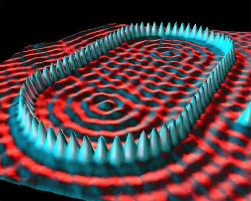
At the very frontier of nano-technology are researchers' endeavors to control and leverage the quantum nature of matter. Unlike the messily analog world we're used to, the quantum world offers the potential of orderly, defined states which can be used for fast and dense calculation and storage. Nanowerk reports on some interesting and rather beautiful work performed at IBM more than a decade ago but newly spotlighted in an art exhibit, of all things, at the United States Patent and Trademark Museum in Alexandria, Virginia:
Driven by their discovery of the STM's ability to image the wave patterns (more precisely known as the "density distribution") of electrons on the surface of a metal, IBM Scientists Michael Crommie, Chris Lutz and Don Eigler (the "artists") were compelled to take the next step -- building an electron's "quantum state" to their own design. Here they have positioned 48 iron atoms into a circular ring in order to "corral" some of the surface electrons and force them into quantum states determined by the circular corral walls. The ripples in the ring of atoms are the wave patterns of some of the electrons that were trapped in the corral. The mechanics-turned-artists were delighted to discover that they could quantitatively account for the behavior of the electrons by solving a classic problem in quantum mechanics -- a particle in a hard-wall box -- paving the way for building functional quantum states for potential use in future computer chips and other areas.More fascinating images and discussion are posted at http://www.almaden.ibm.com/vis/stm/gallery.html
Nanowerk notes,
IBM researchers continue using STM technology in an effort to pave the way for circuits made from atomic and molecular components. Such circuits could enable computers with hundreds of thousands of times more logic elements on a chip than today's state-of-the-art technology. That, in turn, could lead to smaller, faster, lower-power and even more portable computers and devices nobody has even imagined yet.They also provide a nice "timeline of the legacy of IBM's Nobel Prize-winning Scanning Tunneling Microscope":
- 1981: Invention of the STM
- 1986: IBM Researchers Gerd Binnig and Heinrich Rohrer win the Nobel Prize in
physics for inventing the STM- 1990: For the first time, the ability to position individual atoms is
demonstrated by spelling out "I-B-M" using xenon atoms- 1993: Quantum Corrals created
- 1998: Discovery of molecular wheels
- 2000: Discovery of the quantum mirage effect
- 2002: Molecule cascade created
- 2004: Single-atom magnetic measurement achieved
- 2006: Ability to control atomic magnetism achieved
09 August 2007
Note the subscription box down on the right
I set up a free (and spam-free) email thingie which will deliver fresh, steaming Carpe Nano posts directly to your inbox. Yum.
Scroll down to the right.
Scroll down to the right.
Welcome NI Week visitors
The kindly folks who have shepherded NI Week into a hugely-attended monument to networking and collaboration this year have put a link to Carpe Nano up on their daily summary of external coverage of the event. Thanks!
Yesterday's "Industry Experts" panel on Breakthrough Innovation, in which I was so fortunate to participate (and even netted a pre-event press mention), went off well. We had some spirited discussion which I hope was as engaging for the audience as it was for those of us up on the dais. A video of the session will be available Real Soon Now. I'll provide a link when it's up.
-----
UPDATE, 30 Aug. 2007: The Industry Experts video is now online: http://www.ni.com/niweek/keynote_videos.htm -- click on "Industry Experts Panel." More commentary on the panel and conference here.
Yesterday's "Industry Experts" panel on Breakthrough Innovation, in which I was so fortunate to participate (and even netted a pre-event press mention), went off well. We had some spirited discussion which I hope was as engaging for the audience as it was for those of us up on the dais. A video of the session will be available Real Soon Now. I'll provide a link when it's up.
-----
UPDATE, 30 Aug. 2007: The Industry Experts video is now online: http://www.ni.com/niweek/keynote_videos.htm -- click on "Industry Experts Panel." More commentary on the panel and conference here.
"OAI adds nano imprint lithography option for mask aligners"
Here's something clever, and good news for the nascent field of nanoimprint lithography-- the art of forming exceedingly small structures on planar substrates by, well, stamping 'em. The technology allows formation of much smaller and more sharply-defined structures than can be achieved via optical microlithography (the foundation of the semiconductor industry). Besides potentially enabling the semiconductor industry's next act in its methodical trudge along Moore's Law, the technique shows promise for forming useful patterned structures on next-generation disk-drive media and pole features for read-write heads, and for "laboratory on a chip" substrates for biomedical and homeland-security sensing. And it's an enabler for really groundbreaking new devices like the first room-temperature single-electron memory cell developed by Wei Wu at Princeton (where he studied under nanoimprint lithography pioneer Stephen Chou) and now at HP.
Now OAI, a semiconductor microlithography toolmaker, has mashed nanoimprint lithography into its mainstream tools as a swappable option, as reported by Small Times:
A nice solution, a fine differentiator for OAI (whose tools are touted for their flexibility), and a good way for deliberate and risk-averse chipmakers to position themselves to leverage this new technology.
Now OAI, a semiconductor microlithography toolmaker, has mashed nanoimprint lithography into its mainstream tools as a swappable option, as reported by Small Times:
OAI adds nano imprint lithography option for mask aligners
August 1, 2007 -- OAI (Optical Associates Inc.) says that it has added to its mask aligners nano imprint lithography with sub-20 nm resolution. Working with Nanolithosolution Inc. (NLS), OAI is offering a nano imprint module as an option for all of the company's mask aligners -- which can then be used as imprint systems or as standard mask aligners (the module can be easily removed at any time). The module can be included with new orders or retrofit onto existing systems.... OAI's nano imprint module was developed by HP after years of research and development.
A nice solution, a fine differentiator for OAI (whose tools are touted for their flexibility), and a good way for deliberate and risk-averse chipmakers to position themselves to leverage this new technology.
07 August 2007
Y.A.B.A.F.M.I. (Yet another brilliant AFM innovation)
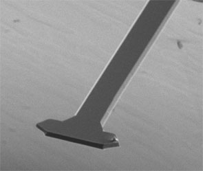
Atomic force microscopy is a leading tool for nanoscale studies of surfaces and objects as small as molecules and even atoms. With nanoscale features commonplace in semiconductor, data storage and life-sciences applications, AFMs are important for both research and industrial uses. These sophisticated instruments build a picture of the nano-world in much the same way that a blind man with a white cane does, using an atomic-sharp tip on a tiny spring cantilever whose motion is observed by sensitive instrumentation. But, as Nanowerk describes, researchers at Harvard and Stanford have literally put a new twist on the conventional way of doing things:
Hmph. I got bit by the non-linear dynamics they're talking about in a customer's advanced AFM application just ten days ago. Not being an atomic force microscopist, at first I had no idea what I was looking at and thought our instrumentation had gone bonkers. Nanowerk and Sahin continue:
"In order to create a high speed and sensitive nanomechanical measurement tool, we have started from the most commonly used AFM technique called the tapping mode" explains [Harvard's Ozgur] Sahin. "The primary advantage of this technique is that it protects the tip and the sample during the imaging process and minimizes the interaction forces.
"For our goal of performing mechanical measurements, tapping mode also provides a unique opportunity because the sharp tip is moving back and forth against the surface and feels the variation of force during the interaction. If one can detect those forces varying with tip sample distance, one can perform a clear and detailed mechanical analysis."
Unfortunately, there are major difficulties in measuring the forces between the tip and the sample. These forces change at a rate much faster than the vibration of the cantilever, therefore the force sensing cantilever cannot respond to them. Indeed, there is a wealth of publications in the literature working on the non-linear dynamics of tapping cantilevers that seek indirect ways to measure these forces.
This is looking like another fundamental advance in a field that's littered with them.
"In a way, our work stands on the 'shoulders of these giants', because they have reached a very good understanding of the complicated cantilever dynamics in AFMs" says Sahin. "Nevertheless, we have taken a different approach by engineering the force sensing cantilever to measure the interaction forces directly."
The AFM cantilever has many vibration modes. Each one of these modes can act as an independent force sensor. The rapidly changing forces demand a fast (high resonance frequency) mode to be used. The problem with high resonance frequency modes is that they are stiff and do not bend easily to give a good signal.
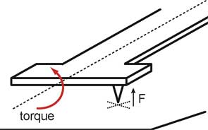
"What we have noticed is that torsional vibration modes allow good signal levels and they have high enough resonance frequencies" says Sahin. "Unfortunately, tip sample forces do not excite torsional oscillations because the conventional cantilevers have their tips on the center line. Therefore, we designed cantilevers that have their tips off-centered. When this cantilever hits the surface, tip-sample forces generate a torque that bends the cantilever torsionally. Torsional vibrations can be detected in a commercial AFM system simultaneously with the vertical vibrations." When this cantilever is operated in conventional tapping-mode – touching the surface ever so lightly some 50,000 times per second (50 kHz) – the torsional vibrations can be simultaneously detected and translated into a time-varying tip-sample force waveform which contains detailed information about the mechanical properties of the sample.
"In principle, the speed of these measurements is limited by the oscillation frequency of the cantilever" says Sahin. "At the moment we are not fully benefiting from the speed enhancement, however, it is still more than a factor of thousand times faster than conventional mechanical measurements, yet it is much gentler to the sample.
"Improved speed enables mapping mechanical properties across a surface with nanometer resolution. I believe that in the near future we will see mechanical measurements performed within a microsecond. This will open up a new window to study time dependent phenomena at the nanoscale, such as protein folding and chemical reactions in general."
06 August 2007
Off to see the wizards
The Austin American-Statesman has a nice preview summary of the NI Week confabulation which commences tomorrow in Austin. I referenced this a few days ago here on Carpe Nano while expanding on the topic of innovation.
The article is really quite a nice set of examples of how innovation can be driven by customers and achieved by artful incrementalism and cross-pollination:
...Actually, I'm not heading the panel, just one o' the guys, but I'll do my best to help make it hop.
The point is: after a good conference, one walks away with (among other things) the germs of new ideas, new ways of doing things, new perceptions on market needs and trends, new contacts with bright folks who can help you do things with a new twist. Played right, those can propel exploration and development in unanticipated directions.
The article is really quite a nice set of examples of how innovation can be driven by customers and achieved by artful incrementalism and cross-pollination:
The article goes on to quote Yours Truly advocating collusion:...because NI Week brings together a large group of LabView's most loyal users, [Omid] Sojoodi, a senior group manager, and [Aljosa] Vrancic, a principal engineer, use it to get feedback on what they've done and what they might do next.
"We'll have closed-door sessions with our power users and talk about some of our products in development," Sojoodi said. "We target our power users, and they really help shape some of the more specific features we add."
Scott Jordan will be one of the more than 2,000 people expected to come to Austin for NI Week. He's director of nanopositioning at Physik Instrumente-USA and one of National Instruments' earliest customers.
Jordan will head a panel called "Breakthrough Innovation" on Wednesday, discussing different ways people have applied National Instruments' technologies. Those sort of interactions make NI Week an annual stop, he said.
"There's a chance to interact, to collide and to collude with your fellow LabView users, and that's huge," he said. "There's nothing like that anywhere else in the industry."
...Actually, I'm not heading the panel, just one o' the guys, but I'll do my best to help make it hop.
The point is: after a good conference, one walks away with (among other things) the germs of new ideas, new ways of doing things, new perceptions on market needs and trends, new contacts with bright folks who can help you do things with a new twist. Played right, those can propel exploration and development in unanticipated directions.
01 August 2007
Cellular Visions: The Inner Life of a Cell
Hat-tip to StudioDaily.com for helping publicize a remarkable animation of life on the nano scale:
Created by XVIVO, a scientific animation company near Hartford, CT, the animation illustrates unseen molecular mechanisms and the ones they trigger, specifically how white blood cells sense and respond to their surroundings and external stimuli.The StudioDaily.com page referenced above has links to high-definition versions of this remarkable video. For blog purposes it was gratifying to find the whole thing posted on YouTube. The conception and content by were by Alain Viel and Robert A. Lue, and the animation was composed by John Liebler/XVIVO. See http://multimedia.mcb.harvard.edu/ for more information.
Virus 'hybrids' can act as nanoscale memory devices
NewScientistTech reports on a fascinating mash-up of viruses and quantum dots (nanoscale spheroids of selected materials including semiconductor atoms which yield remarkable electro-optic properties due to quantum containment effects). This research was performed at the University of California, Riverside, and published in a paper entitled "Microscale memory characteristics of virus-quantum dot hybrids" in Applied Physics Letters.
A new type of memory device has been made by researchers in the US and Italy by attaching individual viruses to tiny specks of semiconducting material called quantum dots. The "hybrid" material could be used to develop biocompatible electronics and offer a cheap and simple way to make high-density memory chips, the researchers say... "Interactions between organic and inorganic particles are quite fascinating," team leader [Mihri] Ozkan told New Scientist. "In our case, finding the memory effect was quite unexpected because each nanoparticle does not have any memory characteristics on its own, but only when connected as a hybrid."Remarkable.
Non-volatile memory
Ozkan and co-workers began by depositing cosahedral cowpea mosaic viruses (CPMV) on quantum dots (made of cadmium selenide and zinc sulphide) using different binding sites on the virus' capsid, or outer shell. CPMV, a plant virus that is harmless to humans, is about 30 nanometres across and consists of a capsid with an RNA core. Next, the researchers embedded the hybrids into a polymer matrix and sandwiched them between two conducting electrodes for testing. They found that each hybrid unit can be operated as a memory device with conductive states that can be switched between high and low, corresponding to a 1 and a 0, by applying a low voltage. These states are "non-volatile", meaning data is stored even when the power is switched off.
Subscribe to:
Posts (Atom)