16 July 2008

A guru on innovation takes note

My "Breakthrough Innovation" co-panelist, Patricia Seybold, has spotlighted my blog posts on HP's memristor and photonic interconnect developments.

Patty's attention is worthy of note, as she has a track record of pegging paradigm shifts in the technology world and guiding organizations to capitalize on them. Savvy strategists listen to her, and successful ones put her advice to work.

Most critical is her relentless focus on customers and her insistence on involving them early in the strategic and developmental process, central to the ecosystem of stakeholders in a commercial endeavor. As she states in her blog's definition of Outside Innovation--both her mantra and the title of one of her books:

What is Outside Innovation?

It’s when customers lead the design of your business processes, products, services, and business models. It’s when customers roll up their sleeves to co-design their products and your business. It’s when customers attract other customers to build a vital customer-centric ecosystem around your products and services. The good news is that customer-led innovation is one of the most predictably successful innovation processes. The bad news is that many managers and executives don’t yet believe in it. Today, that’s their loss. Ultimately, it may be their downfall.

Exactly right. Too many businesspeople are happy to say, "The customer is always right" while missing the opportunity to harness customers' insights early in the strategic or design process when it can have its most profound leverage and produce the most striking competitive advantage. As she notes:

HOW DO YOU WIN IN INNOVATION?
You no longer win by having the smartest engineers and scientists; you win by having the smartest customers!

...And listening to them.

A corollary to that is to seize every opportunity to advance the education--the "smartening"--of your customers. Including: facilitate their learning from each other.

The same goes for the rest of your enterprise's ecosystem. Regardless of your business, one of the most valuable take-aways from HP's purposeful ecosystem-building was illuminated in their Photonics Interconnect Forum when Jamie Beckett quoted HP Labs Director Prith Banerjee: "Not all the smart people work at HP." If so, then the ecosystem-building and customer-smartening is a way of multiplying the ones who work with them.

Call it a positive feedback mechanism for organizational IQ.

16 June 2008

"Fast bipolar nonvolatile switching," and why it changes everything


Yet more memristor news from HP Labs. An eye-blink after their stunning news of discovering the memristor's existence as the fourth fundamental passive electronic circuit element, comes Nature Nanotech's advance online publication of significant progress in the practical fabrication of these devices.

Authors Yang, Pickett, Li, Ohlberg, Stewart and Williams--all of HP Labs in Palo Alto--state:

We have built micro- and nanoscale TiO2 junction devices with platinum electrodes that exhibit fast bipolar nonvolatile switching. We demonstrate that switching involves changes to the electronic barrier at the Pt/TiO2 interface due to the drift of positively charged oxygen vacancies under an applied electric field. Vacancy drift towards the interface creates conducting channels that shunt, or short-circuit, the electronic barrier to switch ON. The drift of vacancies away from the interface annilihilates such channels, recovering the electronic barrier to switch OFF. Using this model we have built TiO2 crosspoints with engineered oxygen vacancy profiles that predictively control the switching polarity and conductance.

The keywords are "engineered oxygen vacancy profiles" and "predictively control." These indicate that memristors are hurtling from their emergence as a laboratory success-story to land square in the everyday IC design toolkit, right before our eyes. Remarkable!

More remarkable is the unusual behavior of these devices. First, there's no doubt that they'll be used as replacements for flash RAM and hard disks: they're faster, they use less energy, they would appear to be denser (50x50nm, in the versions discussed in Nature Nanotech), they operate in parallel, and scalability seems to be a real strength. Given the world's exponentiating appetite for information and information storage, this is all fine news for iPhones and laptops and other good things. But memristors' capability is not limited to storing 1's and 0's. That would be so 21st century. No, memristors can store values in-between. They are analog devices, and they will facilitate parallel analog computers. Those are common enough: you have one between your ears.

HP Labs' Jamie Beckett spoke with the researchers:
"A conventional device has just 0 and 1 – two states – this can be 0.2 or 0.5 or 0.9," says Yang. That in-between quality is what gives the memristor its potential for brain-like information processing... Any learning a computer displays today is the result of software. What we're talking about is the computer itself – the hardware – being able to learn."

Beckett elaborates,
...[Such a computer] could gain pattern-matching abilities [or could] adapt its user interface based on how you use it. These same abilities make it ideal for such artificial intelligence applications as recognizing faces or understanding speech.

Another benefit would be that such an architecture could be inherently self-optimizing. Presented with a repetitive task, or one requiring parallel processing, such a computer could be designed to route subtasks internally in increasingly efficient ways or using increasingly efficient algorithms. Tired of PCs that seem slower after a few months' use than when they were new? This computer would do just the opposite.

Beckett continues:
"When John Von Neumann first proposed computing machines 60 years ago, he proposed they function the way the brain does," says Stewart. "That would have meant analog parallel computing, but it was impossible to build at that time. Instead, we got digital serial computers."
Now it may be possible to build large-scale analog parallel computing machines, he says. "The advantage of those machines is that intrinsically they can do more learning."

Not science fiction. Science fact. And soon--sooner than any of us imagined--it will be up to the engineers and entrepreneurs to leverage this in fantastical ways, using memristors as routinely as they do transistors, invented just sixty years ago.


09 June 2008

Putting the "Lab" back in "LabVIEW" -- while spreading LabVIEW out of the lab


As my panel on "Breakthrough Innovation" at NI Week last year discussed, National Instruments and its LabVIEW programming environment are both an important part of the nanotechnology ecosystem and a fine case study of the commercial benefits of ecosystem-building and customer-driven, recombinant innovation.

So some media coverage of National Instruments caught my eye recently, such as:

National Instruments Announces Global Multi-core Programming Workshop

National Instruments (Nasdaq: NATI) today announced an initiative sponsored by Intel Corporation to deliver free, hands-on multi-core programming workshops based on the NI LabVIEW graphical programming language to engineers and scientists around the globe. The Multi-core Programming with NI LabVIEW Hands-On Workshop will be presented in 18 U.S. and Canadian cities beginning in May and 15 international cities this fall...

and


EETimes: LabView poised for parallel role


James Truchard thinks he may have one of the keys to the multicore era.
The chief executive of National Instruments believes the company's flagship LabView environment offers many of the tools parallel programmers need today. NI has plugged into parallel research efforts at Intel Corp. and Berkeley to make sure LabView evolves with the times...
LabView can automate the assignment of jobs to different cores and threads. It also can generate C code and offers tools to manually optimize CPU loading, debugging and the use of cache in multicore chips...
"This is going to be pretty painful for people," said Truchard. "Today's programming languages really weren't developed for parallel programming" and the new mechanisms Intel and others are developing to plug the holes "add a lot of complexity to the programming environment," he said...
Truchard notes that high school students in the annual First Robotics contest used LabView to program FPGAs. Last year NI set up a lab at Berkeley so students there could use its tools to prototype embedded system designs.

(How about that. High school and college students making their own silicon. Wow.)

The program is one of several at NI aimed at keeping LabView in the forefront of parallel programming research, currently one of the hottest topics in computer science, thanks to the move to multicore processors...

As you can deduce, there has been angst among analysts and engineers alike about the scarcity of software architectures supporting multiprocessing and parallelism.

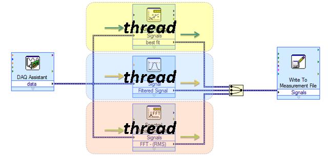
Hardware has gotten ahead of software. But NI has had parallelism nailed in the architecture of LabVIEW for more than two decades, at least for scientific instrumentation and process automation. With the introduction of LabVIEW FPGA three years ago and LabVIEW 8.5 for multicore processors last year, support for true parallelism became not only possible but easy.

Now comes this "initiative sponsored by Intel."

The thing that raised my antennas is that the coverage underplays LabVIEW's traditional market focus on scientific instrumentation and process automation.

Is NI staging a breakout into general computing? Might LabVIEW be the new C++? Is NI taking the "Lab" out of "LabVIEW"?

Technically, there's no reason it couldn't happen. It is a fully-fledged programming environment.

If, say, The MathWorks issued a press release about Matlab, touting sponsorship by Intel, extolling multiprocessing support, commencing a worldwide tour that spotlights the ease with which parallelism can be leveraged and managed on its platform ...and avoiding mention of its foundational calculational capabilities... then we might all agree that would be news. And so is this.

So. Can they take LabVIEW out of the lab? Is that what this is about, even? Maybe I'm just running a fever, but that's how it hit me.

If I were to venture a suggestion, I'd advise that NI consider seeding the programming world with a version of LabVIEW that omits its instrumentation and heavy-duty numerical modules. Maybe even a free one, or one targeted at students. Include its current facilities for integrating traditional code, and watch what happens when folks realize how straightforward programming for multiprocessing can be.

Arguing against the notion is the dictum from page 102 of Scott's Big Book of Pithy Pronouncements: "The Great Unfunded Liability of technology is: Support." On the other hand, NI's experience with Lego Robotics might suggest an affordable upper bound for the incremental support-cost obligation.

The time is right for Dr. T to stake his claim as the Moses of Multiprocessing. He already has the stone tablets. (He got 'em from Jeff Kodosky.)


Happily, research customers can revel in another new initiative at NI, aimed at strengthening its traditional ties to the academic and research marketplaces. (After all, another dictum is, "Dance with the girl that brought ya.") I don't know all the details yet, but what I've heard is exciting for researchers at colleges and universities. It includes an NI Week Academic Forum, a focused day of presentations and discussions for research customers and industry partners, which extends NI Week one day forward. More at http://www.ni.com/niweek/academic.htm --and it appears you'll be hearing more about the broader aspects of this new outreach initiative in the coming weeks.


P.S. I learned today that my "Breakthrough Innovations" co-panelist, Dr. Andrew Hargadon, Director of the Center for Entrepreneurship and the Energy Efficiency Center at the University of California, Davis, will present the closing keynote address at this summer's NI Week. Excellent!

----------

UPDATE: 2 July 2008: The Mystery of the Exploding Hit-Meter has been solved, thanks to a kindly email from NI's Vincent Carpentier. Seems this post is linked in NI News for July '08. The whole newsletter is well worth visiting-- lots of exciting developments and interesting applications, with webcasts and other resources of interest to both LabVIEW users and just-plain-folks interested in the latest in computing and instrumentation.

15 May 2008

Optical communications goes nano -- HP announces practical interconnect tech (and an ecosystem for it to grow in)

Pretty much everyone in developed countries appreciates the escalating appetite for bandwidth of our indispensible digital companions. Phil Edholm of Nortel posted an intriguing graphic recently which shows both historic and projected per-user bandwidth consumption and compares these to other noted growth laws:


...Note the ramp-ups corresponding to adoption of new applications and media such as personal audio (MP3s) and streaming video. (And let's not forget VOIP. And I would personally add escalating adoption of desktop virtual machines to the mix, though few analysts seem to recognize that as a trend yet.) Edholm is the gentleman who exposited bandwidth's equivalent to the semiconductor industry's Moore's Law, reducing its exponentiation to sensible (and highly predictable) form:


The skyrocketing consumption of Internet bits is easy enough to appreciate. But also ponder what this means for the internal communications bandwidth of the devices themselves. Horsing all that data around requires not only better connectivity and more storage and processing power, but also higher internal communications throughput and more flexible and complex routing. But at the same time, chips are getting smaller and denser, buses grow wider, and clock-rates increase (for both performance and marketing reasons).

The physics of these realities quickly collide. Signal integrity, dielectric losses, routing skew, cross-talk, power consumption... nightmares pile on nightmares for circuit engineers trying to move data where it needs to be and when, inside chips and between them, and between the boards they live on. How to meet tomorrow's needs?

One way would be to use optical interconnects, the workhorse of long-haul, high-volume telecommunications. But costs have blocked that. A few short years ago, EDN noted:

...optical interconnects are likely to displace copper only in buses and networks that route signals over distances greater than tens of feet. The reasons are economic. SI experts indicate that the cost of implementing shorter interconnects with optics is at least an order of magnitude greater than that of using copper and the silicon devices that drive it. In fact, typical optical-to-copper cost ratios are probably closer to 100-to-1. Indeed, one SI manager, despite forecasting its decline, suggests that the cost ratio might currently be as high as 10,000-to-1.
O, ye of little faith. That sets the stage nicely for the latest news from HP Labs, which is just rocking with innovations lately. As reported in EE Times:


Using silicon photonics to connect blades, boards, chips and eventually cores on the same chip has become a strategic goal for Hewlett Packard... By harnessing its expertise in nanoimprint lithography to fashion low-cost, high-speed silicon photonic devices, HP said it hopes to seed the fledgling community of optical interconnect component makers. Rather than doing it all, HP is seeking partners with other silicon photonic pioneers in hopes of developing its first optical interconnect technology in products by 2009.

Most reportage skips right over that important point. So let's pause for a moment and relate this back to a topic of some earlier posts (in particular this one) regarding the panel discussion on "Breakthrough Innovation" I was honored to join last summer. Here we have a team of galactic-class innovators... and they're not locking it up. Instead, they're building a community to make more breakthroughs happen faster. HP's CTO Terry Morris even uses one of my favorite innovation-related words, see if you can pick it out:

"Our business strategy is to pull parters along and build a community that benefits from the intellectual property at HP Labs--a community that provides the ecosystem to enable the delivery of photonic interconnects in volume."
Exactly on-target. Morris is channeling my co-panelists Patricia Seybold and Andrew Hargadon. They've studied innovation and have shown this is how breakthroughs are nurtured in savvy organizations.

EE Times continues:

HP described its laboratory demonstrations of the components needed for creating optical interconnects that handle communication among systems and boards... Its free-space optical connection provided a 240 Gbit/s optical connection that beamed information through the air between boards. Researcher also described a MEMS micro-lens scanner fabricated from silicon-on-insulator that focuses between-board lasers.
(Digression: That brings up topic dear to mine own heart, as photonic alignment automation is my home field, with a couple patents, a current emphasis on highly optimized microrobotic alignment and production assembly equipment, and a very enjoyable collaboration with some brilliant researchers at MIT who have developed a six-degree-of-freedom silicon MEMs nanopositioner ideal for embedded micro-optical tasks (see #6466-24 at the link, also this). Exciting work continues there; meanwhile we were able to implement both Hyperbit (allowing smaller/cheaper DACs to be used) and Convolve, Inc.'s always-amazing Input Shaping(R) technology (to eliminate motion-generated vibration without the complexity of a closed-loop implementation). The six-DOF control was implemented in an FPGA using LabVIEW and updated all six axes simultaneously at 10kHz. Here are some micro-scale laser vibrometry videos on YouTube (metrology courtesy of Polytec) which show the impact of what we accomplished, showing a square-wave input to the speck-sized MEMS hexapod, with metrology in the velocity domain: before and after-- the improvement in resolution, controllability and stability is dramatic. The MIT MicroHexFlex MEMS nanopositioner is a marvelous platform for embedded micro-optical pointing and coupling optimization.)
Back to HP's insightful plans. Another ingredient of Hargadon's observations of the innovation process is combinatorial leveraging of technologies from other fields. In this case, one example is the venerable concept of embossing. That's basically what nanoimprint lithography is all about. And it's key to burying the cost issues of small-scale photonic interconnects once and for all:

Instead of using telecommunications-type photonics--which is designed for 300 meter ranges--HP said it wants to craft a family of low-power signaling technologies that use silicon nanoimprint lithography to fashion low-cost alternatives for optical communnications.

Fascinating. And one of the more impressive aspects of HP's news is the breadth and depth of their nanoimprint-based toolkit. The demonstrations included:
...cheap plastic waveguides, micro-lenses and beamsplitters [allowing demonstration of] a 10-bit-wide optical data bus that used just 1 milliwatt of laser power to interconnect eight different modules at 10 Gbit/s/channel for an aggregate bandwidth of over 250 Gbit/s. "What we are working toward now are novel optical connections, such as board-to-board connections using a photonic bus that enables us to replace an 80-watt chip that performs the electronic switching function today with a molded piece of plastic," said Morris [including] a silicon ring resonator that it hopes to fashion with imprint lithography. "HP Labs has already demonstrated one of the world's smallest and lowest power silicon ring resonators. Now we want to show how to do it with nanoimprint lithography because a dense pattern that takes 60 hours to create with e-beam lithography could take only 30 minutes for nanoimprint lithography," Morris claimed.

And unlike many nanotechnologies, this development seems well-grounded and commercializable in the near term:


HP contends that its photonic interconnects are poised for commercialization, which will begin immediately along with business partners. In addition to HP's university partners, over a dozen companies attended the HP forum, including Avago, Corning, Intel and Lightwire. The goal is to develop "the infrastructure to get photonic interconnects to market," said Morris. "We already have photonic waveguides that can operate at up to terahertz ranges. Now we want to make sure that our solutions work in real computing environments," said Morris.

The potential impact is sweeping in scope, encompassing "...all communications in the range of 100 nanometers on a chip all the way up to 100 meters between systems." You'll see this in both existing and new applications:


"In the near term we want to connect boards and blades with photonic interconnects. In the long-term we want to build on-chip photonic connections which we think will break the core-to-memory bottleneck... Instead of going through a switch and out onto a congested bus then back through the switch, we plan on adding inexpensive direct connections that add a dimension of connectivity not possible today," said Morris. "For instance, we could add photonic connections between blades for true 3D meshes and toroids, while remaining within the confines of existing board infrastructures."

With its big memristor news of a few days ago, that's HP's second development in a week enabling radically new computing architectures with dramatic cost and power savings. Let's hope they keep it up.

Full disclosure: I'm an HP shareholder. And after I read about this development, I bought more.

06 May 2008

Another insight into memristors


Thomas Kraemer has a nice alternative diagram of where the memristor (about which I blogged yesterday) fits in the compact constellation of passive circuit elements. By placing Voltage at the center of a triangle, some nice symmetry is revealed.

I'm having a bit of trouble getting the linked image of Kraemer's diagram to post here, so if it doesn't show up above, please visit the link to Kraemer's post.

05 May 2008

True news from H-P-- memristor nano-memory element

Seems Berkeley might be hanging a new Nobel plaque above some mantel soon.

37 years ago, Dr. Leon Chua, a professor in the University of California's Electrical Engineering and Computer Sciences Department, noticed an unfilled symmetry between fundamental electromagnetic equations relating charge and flux and their corresponding passive circuit elements. He filled this blank with a conjectural passive element he termed a memristor, a device with a hysteretic (history-dependent) behavior that changes its electrical characteristics based on past current-flow history:

(Image courtesy of IEEE Spectrum's superb article on the topic.)

Chua showed that such a circuit-element could be kludged for demonstration purposes with a handful of commonplace components, but actual memristors have not been seen in the wild. Or, at least, recognized... until now, thanks to insightful work, published this month in Nature, by R. Stanley Williams, Greg Snider, Dmitri Strukov and Duncan Stewart, all of HP Labs in Palo Alto. (Williams is director of HP's Information and Quantum Systems Lab).

Turns out memristors have been created before but were unrecognized until very recently:

“People have been reporting funny current voltage characteristics in the literature for 50 years,” Williams says. “I went to these old papers and looked at the figures and said, ‘Yup, they've got memristance, and they didn't know how to interpret it.' ”

Louis Pasteur noted, "Chance favors the prepared mind," but sometimes it's the hair-raising strangeness a person encounters that sets them off on a voyage of discovery... and innovation:

...Williams and his group were working on molecular electronics when they started to notice strange behavior in their devices. “They were doing really funky things, and we couldn't figure out what [was going on],” Williams says. Then [Snider] rediscovered Chua's work from 1971. “He said, ‘Hey guys, I don't know what we've got, but this is what we want,' ” Williams remembers. Williams spent several years reading and rereading Chua's papers. “It was several years of scratching my head and thinking about it.” Then Williams realized their molecular devices were really memristors. “It just hit me between the eyes.”

And guess what, it's "green." Since the memristor's memory effect is a fundamental physical property of its construction, it heralds an era when ultra-fast information storage can be implemented on a massive scale yet consume no power except when being read or written. Contrast that with today's spinning hard disks, power-inefficient DRAM, and then reflect on the electrical appetite of something like a server farm. For example, consider Google's new site in The Dalles, Oregon: 108 Megawatts according to a hysterical Harper's, "enough to power 82,000 homes," to serve up things like "a query on 'American Idol'," a top search on Google News in 2007. Or, for a less-Luddite example than Harper's hectoring screed, consider that the sale of 20 million digital picture frames has been projected this year, each consuming about 15 Watts... 300 Megawatts! No doubt Harper's outraged author, Ginger Strand, could write a whole tract about how many warm, healthful vegan breakfasts could be cooked for starving children instead... but consider that memristors could eliminate a large chunk of both examples' power usage. Technology--and capitalism--is both the problem and the solution.

And, in case it's not already obvious from the figures and discussion so far, the discovery of demonstrable (and manufacturable) memristors is a feat of nanotechnology:

...Memristance as a property of a material was, until recently, too subtle to make use of. It is swamped by other effects, until you look at materials and devices that are mere nanometers in size. No one was looking particularly hard for memristance, either. In the absence of an application, there was no need. No engineers were saying, “If we only had a memristor, we could do X,” says [Columbia University electrical engineering professor David] Vallancourt. In fact, Vallancourt, who has been teaching circuit design for years, had never heard of memristance before this week.

Well done, gentlemen.

Practical implementation seems to be within grasp:

HP Labs is now working out how to manufacture memristors from TiO2 and other materials and figuring out the physics behind them. They also have a circuit group working out how to integrate memristors and silicon circuits on the same chip. The HP group has a hybrid silicon CMOS memristor chip “sitting on a chip tester in our lab right now,” says Williams.

But the novel behavior of memristors might open the door to entirely new computing paradigms:

In fact, he hopes to combine memristors with traditional circuit-design elements to produce a device that does computation in a non-Boolean fashion. “We won't claim that we're going to build a brain, but we want something that will compute like a brain,” Williams says. They think they can abstract “the whole synapse idea” to do essentially analog computation in an efficient manner. “Some things that would take a digital computer forever to do, an analog computer would just breeze through,” he says.

Wow. Optimism about the world ahead absolutely flows from nanotechnology. I live amid this stuff every day, and it never ceases to amaze me.

If Ginger Strand wants to pillory society's puerile fascination with American Idol, she might consider urging an episode of Idol devoted to Williams, Snider, Strukov, Stewart and Chua instead.

04 May 2008

Resuming the festivities


The world of nanotechnology doesn't hold still, but neither does life. Not long after my last post, my wife was diagnosed with a brain tumor. Fortunately we have awesome medical resources here in the U.S., and the neurosurgeon to whom we were referred (Dr. Kenneth Blumenfeld) was not only right in our neighborhood, he was regarded very highly by friends in the medical community whom we deeply trust. "He's the very best," one source advised. "Meet him and see what you think. If you're comfortable, there is no reason for shopping around." Remarkable advice, considering we'd expected to consult with Stanford Medical School and the University of California, San Francisco medical school (by all accounts, the absolute citadel of brain medicine), both of which are a stone's throw from us.

The MRIs showed that the tumor was about the size of a racquetball, and from its conformation we had hope that it would not be malignant. The surgery commenced just five days after first identification of the problem.

The tumor was in a difficult location, under the brain and behind/above her right eye, and the extreme morbidity of conventional surgical techniques would have rendered it inoperable just a few years ago. Now, however, the Stealth Navigation technology from Medtronic allows the surgeon to plan and execute surgery in formerly inaccessible locations with far less invasiveness than was previously the norm. The technology is likened to the global positioning system, and it provides a high-precision 3-D mapping of the tumor, brain and involved structures. The surgeon can strategize and operate blind, yet with sub-millimeter precision. Not quite nanometers, but remarkable nonetheless.

The surgery took eight hours, and she was home on the third post-operative day. The enemy turned out to be a benign meningioma, which is pretty much the kind of tumor you want to have if you're going to have a brain tumor. After a couple of months of recuperation, she's back at work, and gaining strength each week. Through it all, our friends, employers and church community were unbelievably supportive. We feel very blessed.

Much is going on in the field of nanotech, and I look forward to posting more regularly now.