22 February 2010

Fabricating transistors without those pesky junctions and dopants

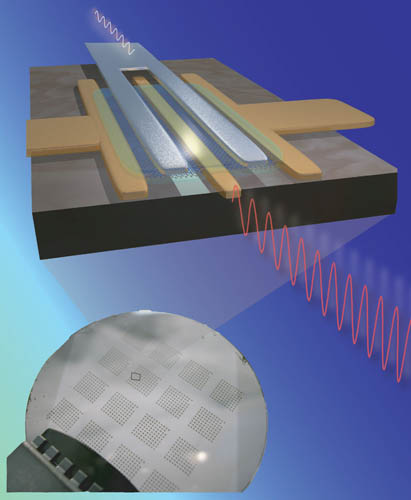
Now this looks interesting. EETimes relates some fascinating research at the Tyndall National Institute in Cork, Ireland: The current flow in nanowires can be pinched off by a simple, conductive nanoscale surrounding structure. According to the EETimes article:

The breakthrough is based on the deployment of a control gate around a silicon wire that measures just a few dozen atoms in diameter. The gate can be used the squeeze the electron channel to nothing without the use of junctions or doping. The development, which could simplify manufacturing of transistors at around the 10-nanometer stage, was created a by a team led by Professor Jean-Pierre Colinge and a paper on the development has been published in Nature Nanotechnology.
It simplifies the production of transistors which also have a near-ideal sub-threshold slope, extremely low leakage currents and less degradation of mobility with gate voltage and temperature than classical transistors, the researchers have claimed. Nonetheless such device can be made to have CMOS compatibility...
"We have designed and fabricated the world s first junctionless transistor that significantly reduces power consumption and greatly simplifies the fabrication process of silicon chips," declared Tyndall's Professor Colinge...

Between these devices, graphene technology and memristors, it would seem that a whole new chapter in integrated-circuit fabrication is in store for the next few years. Somewhere, Gordon Moore smiles.

20 February 2010

Billiard photonics

In another fascinating post to Ars Technica, Chris Lee discusses the leveraging of scattering to improve resolution in a microscope. A more counterintuitive thing is hard to imagine, but he explains...

Scattered photons can make for an improved focus

...a few years ago I reported on a very cool experiment, one that allowed researchers to get a nice focusable beam of light through a scattering medium, such as a sugar cube. This work has been continuing, and there are some technical differences in how the experiment works, but the concepts are still fundamentally the same.
Laser light is shone on a scattering sample, and a tiny fraction of this leaks through, but goes in every direction. To improve the transmission, the researchers place a liquid crystal matrix between the laser and the sample. They modulate the settings on each pixel of the liquid crystal, varying the amount of light transmitted and the effective thickness of each pixel.
Before the liquid crystal, the light beam is a nice smooth thing: the crests, called phase-fronts, of the electromagnetic waves form smooth curves across the profile of the laser beam, as does the intensity of the light. After the liquid crystal, the beam is a complete mess, with the phase-fronts forming some jagged pattern.
It just so happens that the phase-fronts can be chosen so that they exactly compensate for the presence of the scattering sample. This allows some small fraction of the light to pass unhindered through the sample, as if neither the liquid crystal or the sample were there.
Unfortunately, you never really know in advance what the phase-fronts need to look like in order to compensate for the scattering. So you place a CCD camera just after the sample, and then adjust the LCD pixels until you get as bright a dot as possible on the camera sensor. It turns out that this is easy—you just need to take each liquid crystal pixel and adjust it until maximum brightness is achieved. No iteration is needed.


(...Seems to me that if the characteristics of the scattering medium could be more predictable and consistent than the sugar-cube example, the diffraction pattern could be pre-determined. If so, instead of an LCD array, a calculated or even printed pattern could be used. Perhaps the whole optical train could be diffractive, basically a modified zone-plate configuration. --S.J.)


This approach is quite flexible, because it turns out that you can turn the scattering sample into a lens. Just adjust the liquid crystal pixels until the smallest, brightest dot possible turns up, and you have a lens with a focal distance equal to that of the distance between the sample and the camera.
You can also use this technique to improve the resolution of an imaging system, a technique called structured illumination microscopy. Basically, you distort the phase-fronts so that you get multiple sharp points or lines of focus. Each point of focus is, at best, a factor of two better than achievable with ordinary light. But, a factor of two is better than a poke in the eye with a sharp stick, so we'll take it.
What the researchers in the Nature Photonics paper report is an example of structured illumination microscopy, but they claim a factor of ten improvement over the diffraction limit....


While Lee ultimately figures that a factor-of-two is a likelier improvement for resolution, it seems there may be further seductiveness to the technique. Thinking wildly, perhaps objects embedded in scattering media might be observable using some offspring of this research. That could enable applications ranging from oceanic imaging and sensing to in vivo biological imaging. And what does it say about whether scattering is as randomizing as is ordinarily assumed? Are there quantum-entanglement and cryptographic consequences? I've often wondered if we humans have the feeblest grasp of that thing called "randomness"... what we think is random usually isn't at some level, and our proudest efforts to generate randomness without recourse to natural phenomena are really pretty feeble. I wonder if this research may lead to further humbling in that way.

Gold finger: photonics galore

Chris Lee of Ars Technica provides an insightful analysis of a significant new capability in photonics. What impresses me most about this is how well the stage is set for further development and then industrial implementation through recombination with rapidly emerging industrial technologies. I've clipped a summary below and indicated one such synergy, but you should read the whole thing.

Making an optical switch by drawing lines in gold

...Normally, metals make for horrible nonlinear optics—in part because metals fail at transparency—but, they do have one advantage: lots of free electrons. If you shine light on the metallic surface in just the right way, then the electrons start to respond to the light field by oscillating in sympathy. This oscillation moves along the surface of the metal as something called a surface plasmon polariton—which is jargon for electrons that set up an oscillation that maintains a spatial orientation on the surface of the metal.

These plasmons travel at a much slower speed than light, have a much shorter wavelength, and are confined to the metal's surface. As a result, the electric fields associated with the charge oscillation are quite intense—intense enough, in fact, to drive nonlinear interactions. As a result, metals provide light with quite a good medium for things like four-wave mixing, provided you can get the light into the metal. Plasmons are made for this job because they are essentially light waves traveling along the surface of a metal.
[The researchers] ruled lines on the metal that were about 100nm in width...

(...a barn-door for nanoimprint lithography --S.J.)

and separated by around 300nm (center to center). These lines act to slow down the waves, with the delay depending on how close the plasmon wavelength is to the separation of the lines. This also controls the direction of the emission. Light only exits the structure at the point where the emission from each individual line is in phase with the rest, which depends on the spacing of the lines. But, not every color can find a spacing for which this occurs. In this case, the second of the two emitted waves can't find an emission angle that works for it at all, so the device emits only a single wavelength of light.
So, the end result is that, by ruling lines on the gold surface, you can choose which of the two colors you want generated and which direction it's emitted in. As an added bonus, the lines provide sharp points on the surface, which accumulate charge, resulting in very high electric fields (think of a lightening rod on a building). As a result, the four-wave mixing process becomes more efficient.
What's next? That's hard to say. I know that there are some ideas about how these nonlinear optical processes can be made more efficient, and maybe even useful, using plasmonic surfaces. So we may see some plasmonic optical switching devices. The big selling point in plasmonics is usually sensing, though, so things may go in that direction.

One thing that intrigues about this approach is how it leverages and manages those surface plasmon waves. Note the point Lee mentions about the plasmon waves' shorter-than-light wavelengths, necessitated by their comparatively slow velocity. Their short wavelengths would seem to be a useful property for probing and sensing phenomena and physics on the nanoscale, perhaps providing a new tool to bridge the region between light-based microscopies and electron microscopies, which are limited by the electron's Compton wavelength (on the order of 10^-12 m) in the same way that optics are diffraction-limited by photons' wavelengths. In particular, materials with even slower surface plasmon velocities but still generous free electron populations (which I'd imagine equates to "conductivity," though I'm rusty) would have shorter plasmon wavelengths still. Depending on how far down the process can be driven, things could get really interesting, and really weird.

Single. Best. Customer. Experience. Ever.

Here's a quick note of appreciation to Apple for their extraordinary effort to rectify a minor but recurring annoyance with my beloved, well-traveled, hard-working original-issue MacBook Pro. The details are too long and boring to post, but the elevator summary is: I went to the Los Gatos Apple Store for an appointment to visit the "Genius Bar" with a software question. This is always a treat-- imagine talking face-to-face with folks who actually know their products and can communicate effectively, rather than spending hours on hold to Bangalore waiting for an incomprehensible script-reading troll to not solve your problem. Customer service: what a concept. While there, I almost off-handedly mentioned a hardware issue with the machine, which the justly-termed Genius, Trevor, recalled addressing before when my machine was under warranty. He encouraged me to call AppleCare, although my extended warranty had expired last Summer. Within an hour, Apple had spun up an amazing effort to get to the bottom of the issue. Noel at AppleCare could not have taken better care of me and the resolution could not have been more perfect.

It got me thinking. I first used Macs early in my career to run the first versions of LabVIEW, back in my days at Newport Corporation in 1986 when the Mac was the only GUI machine in town. We accomplished some amazing work on those groundbreaking machines, including:
  • Devising an easy-to-use quality-test workstation which made 100% graphical, six-degree-of-freedom interferometry a tool that any production-line assembler could use. This precipitated an avalanche of assembly tweaks and quality improvements from curious assemblers eager to apply their weekend shade-tree-mechanic skills. All these years later, I remain awed and grateful for their gumption and creativity, and at the role LabVIEW and the Mac played in enabling it.

  • Turning around the company's motion-control business segment and turbocharging its instrumentation product lines as the industry's first adopter of National Instruments' brilliant instrument-library initiative for LabVIEW. To show this off, we bravely built a simple virtual instrument from our company's optical hardware and put it on the trade-show floor of the next major conference. It was mobbed. I recall standing in the back of the booth with my boss, the much-missed Dean Hodges, and observing a stunning phenomenon: customers over 35 were looking at the optical hardware, while customers under 35 were looking at the Mac. In a stroke, the Mac had helped us open a highly differentiating dialog with the up-and-coming Young Turks of the laser/electro-optic industry. (An exercise for the user: what would generate a similar effect for your company today?)

  • Building a thriving systems business on technical innovations that LabVIEW on the Mac let us explore quickly and with little risk. The keystone was my work on the first digital gradient search algorithm for nanoscale alignments of optical fibers, waveguides, etc. From idea to first demonstration of that took only a few hours thanks to LabVIEW's dataflow programming paradigm which the Mac's GUI enabled. Eventually we received the very first patent for a LabVIEW-based virtual instrument, and a multi-million-dollar business grew from that seed.
It was an enthralling time, and I even was honored to be subject of a photo interview on "Science and the Mac" in MacWorld magazine. But eventually, Microsoft came out with Windows, and by its version 3.1 there was a version of LabVIEW for it. While my family kept using Macs at home, the world went Windows. And soon we saw how monocultures are a bad thing, both for customers (who are deprived of competition-driven advancements) and for security (having a single, badly-designed lock to pick makes the job easy for the bad guys).

Today, Apple and the Mac are surging again, propelled by superb, imaginative products that are meaningfully differentiated by great performance, compelling design, unmatched solidity and a high-end focus. And please add nonpareil support to that, thanks to a corporate culture that grows Trevors and Noels.

And here, in a ZDNet blog story by David Morgenstern, is terrific news: for scientific and engineering fields, the Mac's story is coming full circle:

Engineering: The Mac is coming back


Most attendees at the Macworld Expo in San Francisco this week — distracted by plentiful iPhone apps, whispered tales of the forthcoming Apple iPad, and the sight of dancing booth workers with their faces covered by unfortunate costumes of gigantic Microsoft Office for Mac icons — may have overlooked a trend: The Macintosh is back in the engineering segment.
Engineering, which was often lumped into the beat called “SciTech,” once was strong segment for the Macintosh. Then in the early 1990s, the platform’s position was weakened and then lost. But now the Mac appears poised for a strong return.
...

“Engineering is primed to take off now [on the Mac],” said Darrin McKinnis, vice president for sales and marketing at CEI of Apex, NC. He said there was a “growing ecosystem of applications” to support Mac engineers and while previously, many engineers purchased Mac hardware to then run Linux applications or even Windows programs in virtualization, his company had seen increasing demand for a native Mac version.
McKinnis pointed to a number of engineering teams around the country that are now almost all working on Macs. With the native Mac apps, the loser will be Linux, he said.
McKinnis has a long (and painful) history with engineering solutions on the Mac. He was once an engineer at the NASA Johnson Space Center in Houston, where in 1995, CIO John Garman decided to eliminate “unnecessary diversity” and switch thousands of Mac workstations over to Windows 95.
The battle was joined between NASA’s directive at the time for Better, Faster, Cheaper,” and what Garman dismissively called “Mac huggers” (a techno-word-play on the “tree huggers” environmentalist sobriquet). It didn’t help that Garman was mentioned in a Microsoft advertisement that thanked customers for their “contributions” to Windows 95.
NASA Mac users tried hard to point out that this policy would cause problems. My MacWEEK colleague Henry Norr wrote a series of articles about the fight to keep the Mac at NASA, which won a Computer Press Association award. Here’s a slice of his Feb. 12, 1996 front page story:
“Making me take a Pentium is like cutting off my right hand and sewing on a left hand,” said a Mac user at NASA’s Johnson Space Center in Houston who recently faced forced migration to Windows. “I’ll learn to use the left hand, but there’s no doubt my productivity is going to suffer, and I’m going to resent it.”
To this engineer and hundreds of other Mac users at the space center, such desktop amputations hardly seem like an effective way to comply with agency administrator Dan Goldin’s much-publicized motto, “Better, Faster, Cheaper.” To them, the space center’s new policy of standardizing on Windows is wasteful, unnecessary and infuriating, and they are not taking it lying down.
Eventually, the fight went to hearings at the Inspector General’s office. McKinnis was one of the staff who testified there. While the investigation concluded with a report that sided with the Mac users, the Mac was supplanted.

No more. The Mac's architectural advantages in performance, security, robustness and ease of use are attracting users snake-bit by the malware, misbehavior and cumbersomeness of Windows and the chaos and geek-intensiveness of the Linux world.

And then there's Trevor and Noel.

14 February 2010

[Yet more] Researchers make faster-than-silicon graphene chips

Egad. A few hours after posting the graphene news from IBM, I encounter this apparently parallel development:

Researchers make faster-than-silicon graphene chips
updated 06:35 pm EST, Wed February 3, 2010
Penn State finds method of making graphene chips

A carbon semiconductor called graphene could replace silicon in computer chips in the near future, researchers at Penn State found. They claim to have developed a way to put the graphene on 4-inch wafers. The Electro-Optics Center Materials Division scientists say their work can eventually lead to chips that are 100 to 1,000 times faster than silicon.


Graphene is a crystalline form of carbon that is made up of two-dimension hexagonal arrays which is ideal for electronic applications. Attempting to place the material onto sheets using the usual methods turns them into irregular graphite structures, however. David Snyder and Randy Cavalero at Penn State say they came up with a method called silicon sublimation that removes silicon from silicon carbide wafers and leaves pure graphene.

A similar process has been used for graphene before, but the EOC is the first group that claims it has perfected the process to a point that lets them produce 4-inch wafers. The smallest wafers using a more conventional method have resulted in 8-inch graphene wafers. Typical wafers used for processors today are roughly 11 inches across. [via EETimes]

A Quantum Leap in Battery Design?

A Quantum Leap in Battery Design
Digital quantum batteries could exceed lithium-ion performance by orders of magnitude.
A "digital quantum battery" concept proposed by a physicist at the University of Illinois at Urbana-Champaign could provide a dramatic boost in energy storage capacity--if it meets its theoretical potential once built.
The concept calls for billions of nanoscale capacitors and would rely on quantum effects--the weird phenomena that occur at atomic size scales--to boost energy storage. Conventional capacitors consist of one pair of macroscale conducting plates, or electrodes, separated by an insulating material. Applying a voltage creates an electric field in the insulating material, storing energy. But all such devices can only hold so much charge, beyond which arcing occurs between the electrodes, wasting the stored power.
If capacitors were instead built as nanoscale arrays--crucially, with electrodes spaced at about 10 nanometers (or 100 atoms) apart--quantum effects ought to suppress such arcing. For years researchers have recognized that nanoscale capacitors exhibit unusually large electric fields, suggesting that the tiny scale of the devices was responsible for preventing energy loss. But "people didn't realize that a large electric field means a large energy density, and could be used for energy storage that would far surpass anything we have today," says Alfred Hubler, the Illinois physicist and lead author of a paper outlining the concept, to be published in the journal Complexity.


That's all quite interesting, and heaven knows the world needs to finally advance beyond battery technology that Volta could understand. Going directly to Hubler's paper yields the following explanation, spanning pgs. 3 and 4:

Nano plasma tubes are generally forward-biased and if the residual gas emits visible light, they can be used for flat-panel plasma lamps and flat panel monitors... The energy density density in reverse-biased nano plasma tubes is small, because gas becomes a partically ionized, conducting plasma at comparatively small electric fields... In this paper, we investitage energy storage in arrays of reverse-biased nano vacuum tubes, which are similar in design to nano plasma tubes, but contain little or no gas... Since there are only residual gases between the electrodes in vacuum junctions, there is no Zener breakdown, no avalanche breakdown, and no material that could be ionized. Electrical breakdown is triggered by quantum mechanical tunneling of electrode material: electron field emission on the cathode and ion field emission on the anode. Because the energy barrier for electron field emission is large and the barrier for ion field emission even larger, the average energy density in reversed-biased nano vacuum tubes can exceed the energy density in solid state tunnel junctions and electrolytic capacitors. Since the inductance of the tubes is very small, the charge-discharge rates exceed batteries and conventional capacitors by orders of magnitude. Charging and discharging involves no faradaic reactions so the lifetime of nano vacuum tubes is virtually unlimited. The volumetric energy density is independent from the materials used as long as they can sustain the mechanical load, the electrodes are good conductors, and the mechanical supports are good insulators. Therefore, nano vacuum tubes can be built from environmentally friendly, non-noxious materials. Materials with a low density are preferable, since the gravimetric density is the ratio between the volumetric energy density and the average density of the electrodes and supports. Leakage currents are small, since the residual gases contain very few charged particles.
The thing is is, I think something much like this has been tried, though not for energy storage: The technology Hubler describes seems very similar to the notion of field-emission displays and surface-conduction electron-emitter displays, two closely-related technologies in which nanoscale vacuum tubes are fabricated microlithograhically and arrayed to stimulate phosphors.


One of Silicon Valley's largest failed ventures was Candescent, a company devoted to developing such displays, which burned through (IIRC) something like $600 million in funding from some stellar sources. As Daniel den Engelsen notes in his article, "The Temptation of Field Emission Displays,"
...Manufacturing of FEDs is too difficult, and thus too expensive; moreover, the recent success of LCDs and PDPs as Flat Panel Displays (FPDs) for TV is now discouraging (large) investments in FED manufacturing facilities. The two main challenges for designing and making FEDs, viz. high voltage breakdown and luminance non-uniformity, are described in this paper. Besides improvements in the field of emitter and spacer technology, a new architecture of FEDs, notably HOPFED, has been proposed recently to solve these two persistent hurdles for manufacturing FEDs.
But energy storage wouldn't care much about luminance non-uniformity, and Hubler seems to have determined that high-voltage breakdown is manageable in his configuration. Hubler and Canon, which acquired the ashes of Candescent from receivership, might want to talk. Sony, a major battery manufacturer as well as a former FED developer, might be another interested party.

Big Blue demos 100GHz chip


Time to rev up this blog thingie again. Lots is going on, including some developments that seem quite practical for commercialization in the not-too-distant future.

Consider, from The Register in England:

Big Blue demos 100GHz chip


IBM reseachers have made a breakthrough in the development of ultra-high-speed transistor design, creating a 100GHz graphene-based wafer-scale device. And that's just for starters.
The transistor that the researchers have developed is a relatively large one, with a gate length of 240 nanometers - speeds should increase as the gate length shrinks.
The field-effect transistor that the IBM team developed exploits what a paper published in the journal Science understates as the "very high carrier mobilities" of graphene, a one-atom-thick sheet of carbon atoms grown on a silicon substrate.
This extraordinarily thin sheet is grown on the silicon epitaxially, meaning that it's created in an ordered crystaline structure on top of another crystaline structure - in this case, good ol' garden-variety silicon.

I wrote about graphene back in the Summer of 2007, noting it seemed more tractable for utilization in manufacturing processes than its more-glamorous siblings, carbon nanotubes. And so it seems: the fact that IBM's development is based on "garden-variety silicon" is a wonderful testament to recombinant innovation and promises practical adoption before too long. It seems hackneyed and threadworn to haul out Moore's Law one more time, but here it is again, keeping pace.