30 August 2007

Changing the world, one electron at a time


Nanosolar is a fascinating company and a venture to watch. Well-funded (in part by some of the guys who brought you Google), with almost 700,000 square feet (65,000 square meters) of fresh manufacturing space, this company has figured out how to leverage self-assembling nanoscale materials to create flexible, printable solar cells of high efficiency and attractive durability and cost. While some credible detractors like Cypress Semiconductor's T.J. Rodgers have their money on more mature silicon-based technologies rather than newer materials like Nanosolar's Copper Indium Gallium Diselenide [CIGS], the sheer coolness of what Nanosolar has accomplished makes it a standout.

There's another reason to cheer Nanosolar: they're doing their manufacturing in the San Francisco Bay Area. With the US dollar held down as a strategy for turbocharging the export economy, this is a fine strategy for a fast path to profitability today, and a welcome boost for the Bay Area's fading manufacturing fortunes.
They're not alone in pursuing novel approaches to solar energy or even flexible solar cells, but Nanosolar seems well-positioned to succeed in the perilous jump from venture to enterprise.
Patricia Seybold on the "Breakthrough Innovations" panel

Patty Seybold has a detailed and perceptive post on her Outside Innovation blog regarding the NI Week Industry Experts panel on "Breakthrough Innovation", on which I was honored to serve with her:


NI’s customers are scientists and engineers who are experts in a wide array of disciplines, from nanotechnology and photo-optics to the design of alternative energy power supplies in automobiles, the control of robots and other manufacturing processes, to the design of signal processing systems on programmable embedded chips in today’s cell phones.

These engineers and scientists use NI’s virtual instrumentation software innovation toolkit, LabVIEW, to design, prototype, and deploy applications that measure real world phenomena—analog signals and physical movement—analyze these signals, describe actions that need to be taken, send out the signals to execute those actions (usually in parallel), analyze the results, and take additional actions. Whether the device being programmed is a nanorobot being used to splice genes or a spectrum analyzer being used to measure radio frequency interference, the scientist is dealing with real world phenomena in real time.

Hanging out with these real world scientists and engineers got me thinking about the future of programming as we know it today. The future of programming is a topic to which NI’s top executives have also been giving a lot of thought.
Yes, they have-- over more than two decades, starting with the very fundament of LabVIEW. So it is considerably ahead of the game in programming's new world of parallelism (concurrency) enabled by multicore processors, which are now at the heart of almost every new personal computer sold. The ability of processes to execute truly in parallel poses all sorts of new possibilities... plus big challenges for programmers who aren't so fortunate as to be using LabVIEW, which is inherently parallel.

As pundits from Bill Gates on down have opined, parallelism poses a potentially bigger revolution in software design than object-oriented programming did. Some of these same folks contend it'll be a decade before programming tools catch up. Theirs, maybe.

As a guru on innovation, Seybold recognized an important comment from LabVIEW inventor Dr. Jeff Kodosky:

“We have a successful parallel language for multicore machines today. You can exploit the performance of multicore machines now. The ultimate architecture for parallel programming is the FPGA (Field Programmable Gate Array) and, of course, LabVIEW is already there,” Jeff Kodosky exclaimed.

That underscores a key point that is often underplayed and under-appreciated: in one smooth move three years ago, LabVIEW wrenched the reconfigurability and raw parallel-processing power of Xilinx's top-end FPGAs from the hands of specially-trained engineers and placed these capabilities in the end-user's hands. No longer just field-programmable, thanks to LabVIEW FPGAs are user-programmable.

In my own native field of scientific instrumentation, this is a truly momentous development. My customers and colleagues will discovering new things this enables for years to come.

My own first FPGA application was to fashion an easy-to-use LabVIEW interface to an instrument whose speed otherwise would have required a custom logic circuit. Next came a controller for a novel MEMS nanopositioner from MIT that implemented my patented DAC-resolution enhancement technology, HyperBit™ and Convolve, Inc's remarkable vibration-cancelling Input Shaping® technology, all operating in six degrees of freedom simultaneously. Next came a high-speed multi-axis analog interface to a nanopositioning controller that didn't have one. Next came some contributions to a customer's novel fast controls for... well, I probably shouldn't say since publication is still pending, but it involves manipulating molecules and measuring forces on a sub-sub-nanometer scale.

...Did I mention those were all done with the same NI card, with reusable, modular code that could be emailed around and ported from application to application just by dropping an icon in and wiring it together? These applications were previously unapproachable without a major custom hardware/software design effort. I did each of 'em at my desk in a few hours. Or on airplanes. Or on my lap-- I implemented HyperBit™ on the FPGA one evening while relaxing on my couch.

Spinning multiple parallel processes on an FPGA is easy, and now multicore processors offer some of the same capabilities as a standard feature of new PCs. That, folks, is a revolution.

A video of the Industry Experts panel on "Breakthrough Innovation" can be viewed at http://www.ni.com/niweek/keynote_videos.htm -- click on "Industry Experts Panel." All the keynotes make for fascinating watching and are recommended.

17 August 2007

Pretty much the limiting case for nanotechnology


At the very frontier of nano-technology are researchers' endeavors to control and leverage the quantum nature of matter. Unlike the messily analog world we're used to, the quantum world offers the potential of orderly, defined states which can be used for fast and dense calculation and storage. Nanowerk reports on some interesting and rather beautiful work performed at IBM more than a decade ago but newly spotlighted in an art exhibit, of all things, at the United States Patent and Trademark Museum in Alexandria, Virginia:

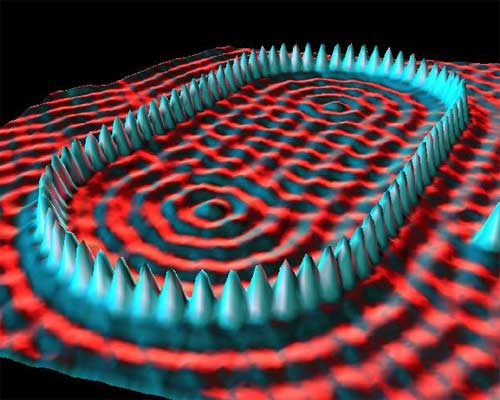
Driven by their discovery of the STM's ability to image the wave patterns (more precisely known as the "density distribution") of electrons on the surface of a metal, IBM Scientists Michael Crommie, Chris Lutz and Don Eigler (the "artists") were compelled to take the next step -- building an electron's "quantum state" to their own design. Here they have positioned 48 iron atoms into a circular ring in order to "corral" some of the surface electrons and force them into quantum states determined by the circular corral walls. The ripples in the ring of atoms are the wave patterns of some of the electrons that were trapped in the corral. The mechanics-turned-artists were delighted to discover that they could quantitatively account for the behavior of the electrons by solving a classic problem in quantum mechanics -- a particle in a hard-wall box -- paving the way for building functional quantum states for potential use in future computer chips and other areas.
More fascinating images and discussion are posted at http://www.almaden.ibm.com/vis/stm/gallery.html

Nanowerk notes,

IBM researchers continue using STM technology in an effort to pave the way for circuits made from atomic and molecular components. Such circuits could enable computers with hundreds of thousands of times more logic elements on a chip than today's state-of-the-art technology. That, in turn, could lead to smaller, faster, lower-power and even more portable computers and devices nobody has even imagined yet.
They also provide a nice "timeline of the legacy of IBM's Nobel Prize-winning Scanning Tunneling Microscope":

  • 1981: Invention of the STM
  • 1986: IBM Researchers Gerd Binnig and Heinrich Rohrer win the Nobel Prize in
    physics for inventing the STM
  • 1990: For the first time, the ability to position individual atoms is
    demonstrated by spelling out "I-B-M" using xenon atoms
  • 1993: Quantum Corrals created
  • 1998: Discovery of molecular wheels
  • 2000: Discovery of the quantum mirage effect
  • 2002: Molecule cascade created
  • 2004: Single-atom magnetic measurement achieved
  • 2006: Ability to control atomic magnetism achieved

09 August 2007

Note the subscription box down on the right

I set up a free (and spam-free) email thingie which will deliver fresh, steaming Carpe Nano posts directly to your inbox. Yum.

Scroll down to the right.

Welcome NI Week visitors

The kindly folks who have shepherded NI Week into a hugely-attended monument to networking and collaboration this year have put a link to Carpe Nano up on their daily summary of external coverage of the event. Thanks!

Yesterday's "Industry Experts" panel on Breakthrough Innovation, in which I was so fortunate to participate (and even netted a pre-event press mention), went off well. We had some spirited discussion which I hope was as engaging for the audience as it was for those of us up on the dais. A video of the session will be available Real Soon Now. I'll provide a link when it's up.

-----

UPDATE, 30 Aug. 2007: The Industry Experts video is now online: http://www.ni.com/niweek/keynote_videos.htm -- click on "Industry Experts Panel." More commentary on the panel and conference here.

"OAI adds nano imprint lithography option for mask aligners"

Here's something clever, and good news for the nascent field of nanoimprint lithography-- the art of forming exceedingly small structures on planar substrates by, well, stamping 'em. The technology allows formation of much smaller and more sharply-defined structures than can be achieved via optical microlithography (the foundation of the semiconductor industry). Besides potentially enabling the semiconductor industry's next act in its methodical trudge along Moore's Law, the technique shows promise for forming useful patterned structures on next-generation disk-drive media and pole features for read-write heads, and for "laboratory on a chip" substrates for biomedical and homeland-security sensing. And it's an enabler for really groundbreaking new devices like the first room-temperature single-electron memory cell developed by Wei Wu at Princeton (where he studied under nanoimprint lithography pioneer Stephen Chou) and now at HP.

Now OAI, a semiconductor microlithography toolmaker, has mashed nanoimprint lithography into its mainstream tools as a swappable option, as reported by Small Times:
OAI adds nano imprint lithography option for mask aligners

August 1, 2007 -- OAI (Optical Associates Inc.) says that it has added to its mask aligners nano imprint lithography with sub-20 nm resolution. Working with Nanolithosolution Inc. (NLS), OAI is offering a nano imprint module as an option for all of the company's mask aligners -- which can then be used as imprint systems or as standard mask aligners (the module can be easily removed at any time). The module can be included with new orders or retrofit onto existing systems.... OAI's nano imprint module was developed by HP after years of research and development.

A nice solution, a fine differentiator for OAI (whose tools are touted for their flexibility), and a good way for deliberate and risk-averse chipmakers to position themselves to leverage this new technology.

07 August 2007

Y.A.B.A.F.M.I. (Yet another brilliant AFM innovation)


Atomic force microscopy is a leading tool for nanoscale studies of surfaces and objects as small as molecules and even atoms. With nanoscale features commonplace in semiconductor, data storage and life-sciences applications, AFMs are important for both research and industrial uses. These sophisticated instruments build a picture of the nano-world in much the same way that a blind man with a white cane does, using an atomic-sharp tip on a tiny spring cantilever whose motion is observed by sensitive instrumentation. But, as Nanowerk describes, researchers at Harvard and Stanford have literally put a new twist on the conventional way of doing things:

"In order to create a high speed and sensitive nanomechanical measurement tool, we have started from the most commonly used AFM technique called the tapping mode" explains [Harvard's Ozgur] Sahin. "The primary advantage of this technique is that it protects the tip and the sample during the imaging process and minimizes the interaction forces.
"For our goal of performing mechanical measurements, tapping mode also provides a unique opportunity because the sharp tip is moving back and forth against the surface and feels the variation of force during the interaction. If one can detect those forces varying with tip sample distance, one can perform a clear and detailed mechanical analysis."
Unfortunately, there are major difficulties in measuring the forces between the tip and the sample. These forces change at a rate much faster than the vibration of the cantilever, therefore the force sensing cantilever cannot respond to them. Indeed, there is a wealth of publications in the literature working on the non-linear dynamics of tapping cantilevers that seek indirect ways to measure these forces.
Hmph. I got bit by the non-linear dynamics they're talking about in a customer's advanced AFM application just ten days ago. Not being an atomic force microscopist, at first I had no idea what I was looking at and thought our instrumentation had gone bonkers. Nanowerk and Sahin continue:

"In a way, our work stands on the 'shoulders of these giants', because they have reached a very good understanding of the complicated cantilever dynamics in AFMs" says Sahin. "Nevertheless, we have taken a different approach by engineering the force sensing cantilever to measure the interaction forces directly."
The AFM cantilever has many vibration modes. Each one of these modes can act as an independent force sensor. The rapidly changing forces demand a fast (high resonance frequency) mode to be used. The problem with high resonance frequency modes is that they are stiff and do not bend easily to give a good signal.
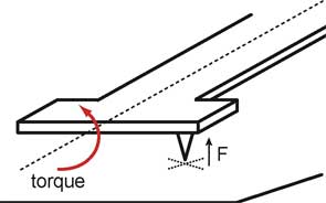
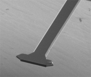
"What we have noticed is that torsional vibration modes allow good signal levels and they have high enough resonance frequencies" says Sahin. "Unfortunately, tip sample forces do not excite torsional oscillations because the conventional cantilevers have their tips on the center line. Therefore, we designed cantilevers that have their tips off-centered. When this cantilever hits the surface, tip-sample forces generate a torque that bends the cantilever torsionally. Torsional vibrations can be detected in a commercial AFM system simultaneously with the vertical vibrations." When this cantilever is operated in conventional tapping-mode – touching the surface ever so lightly some 50,000 times per second (50 kHz) – the torsional vibrations can be simultaneously detected and translated into a time-varying tip-sample force waveform which contains detailed information about the mechanical properties of the sample.
"In principle, the speed of these measurements is limited by the oscillation frequency of the cantilever" says Sahin. "At the moment we are not fully benefiting from the speed enhancement, however, it is still more than a factor of thousand times faster than conventional mechanical measurements, yet it is much gentler to the sample.
"Improved speed enables mapping mechanical properties across a surface with nanometer resolution. I believe that in the near future we will see mechanical measurements performed within a microsecond. This will open up a new window to study time dependent phenomena at the nanoscale, such as protein folding and chemical reactions in general."
This is looking like another fundamental advance in a field that's littered with them.

06 August 2007

Off to see the wizards

The Austin American-Statesman has a nice preview summary of the NI Week confabulation which commences tomorrow in Austin. I referenced this a few days ago here on Carpe Nano while expanding on the topic of innovation.

The article is really quite a nice set of examples of how innovation can be driven by customers and achieved by artful incrementalism and cross-pollination:

...because NI Week brings together a large group of LabView's most loyal users, [Omid] Sojoodi, a senior group manager, and [Aljosa] Vrancic, a principal engineer, use it to get feedback on what they've done and what they might do next.

"We'll have closed-door sessions with our power users and talk about some of our products in development," Sojoodi said. "We target our power users, and they really help shape some of the more specific features we add."

The article goes on to quote Yours Truly advocating collusion:

Scott Jordan will be one of the more than 2,000 people expected to come to Austin for NI Week. He's director of nanopositioning at Physik Instrumente-USA and one of National Instruments' earliest customers.

Jordan will head a panel called "Breakthrough Innovation" on Wednesday, discussing different ways people have applied National Instruments' technologies. Those sort of interactions make NI Week an annual stop, he said.

"There's a chance to interact, to collide and to collude with your fellow LabView users, and that's huge," he said. "There's nothing like that anywhere else in the industry."


...Actually, I'm not heading the panel, just one o' the guys, but I'll do my best to help make it hop.

The point is: after a good conference, one walks away with (among other things) the germs of new ideas, new ways of doing things, new perceptions on market needs and trends, new contacts with bright folks who can help you do things with a new twist. Played right, those can propel exploration and development in unanticipated directions.

01 August 2007

Cellular Visions: The Inner Life of a Cell


Hat-tip to StudioDaily.com for helping publicize a remarkable animation of life on the nano scale:

Created by XVIVO, a scientific animation company near Hartford, CT, the animation illustrates unseen molecular mechanisms and the ones they trigger, specifically how white blood cells sense and respond to their surroundings and external stimuli.
The StudioDaily.com page referenced above has links to high-definition versions of this remarkable video. For blog purposes it was gratifying to find the whole thing posted on YouTube. The conception and content by were by Alain Viel and Robert A. Lue, and the animation was composed by John Liebler/XVIVO. See http://multimedia.mcb.harvard.edu/ for more information.

Virus 'hybrids' can act as nanoscale memory devices

NewScientistTech reports on a fascinating mash-up of viruses and quantum dots (nanoscale spheroids of selected materials including semiconductor atoms which yield remarkable electro-optic properties due to quantum containment effects). This research was performed at the University of California, Riverside, and published in a paper entitled "Microscale memory characteristics of virus-quantum dot hybrids" in Applied Physics Letters.

A new type of memory device has been made by researchers in the US and Italy by attaching individual viruses to tiny specks of semiconducting material called quantum dots. The "hybrid" material could be used to develop biocompatible electronics and offer a cheap and simple way to make high-density memory chips, the researchers say... "Interactions between organic and inorganic particles are quite fascinating," team leader [Mihri] Ozkan told New Scientist. "In our case, finding the memory effect was quite unexpected because each nanoparticle does not have any memory characteristics on its own, but only when connected as a hybrid."
Non-volatile memory
Ozkan and co-workers began by depositing cosahedral cowpea mosaic viruses (CPMV) on quantum dots (made of cadmium selenide and zinc sulphide) using different binding sites on the virus' capsid, or outer shell. CPMV, a plant virus that is harmless to humans, is about 30 nanometres across and consists of a capsid with an RNA core. Next, the researchers embedded the hybrids into a polymer matrix and sandwiched them between two conducting electrodes for testing. They found that each hybrid unit can be operated as a memory device with conductive states that can be switched between high and low, corresponding to a 1 and a 0, by applying a low voltage. These states are "non-volatile", meaning data is stored even when the power is switched off.
Remarkable.